Light Exposure Apparatus and Manufacturing Method of Semiconductor Device Using the Same

a technology of light exposure apparatus and manufacturing method, which is applied in the direction of semiconductor/solid-state device testing/measurement, photomechanical apparatus, instruments, etc., can solve the problems of inferior tft characteristics to those of tft formed in a large grain size region, and the difficulty of making the distance between laser irradiation regions exactly the sam

Inactive Publication Date: 2008-06-26
SEMICON ENERGY LAB CO LTD
View PDF9 Cites 17 Cited by
  • Summary
  • Abstract
  • Description
  • Claims
  • Application Information

AI Technical Summary

Benefits of technology

[0040]According to the invention, the following advantages can be given. First, the formation of a marker is not required since a photolithography can be con

Problems solved by technology

However, in a step of conducting laser annealing using a semiconductor film formed over a substrate as an irradiated region using a plurality of lasers, it is difficult to make distances between laser irradiation regions

Method used


Image

  • Light Exposure Apparatus and Manufacturing Method of Semiconductor Device Using the Same
  • Light Exposure Apparatus and Manufacturing Method of Semiconductor Device Using the Same
  • Light Exposure Apparatus and Manufacturing Method of Semiconductor Device Using the Same

Examples


embodiment 1

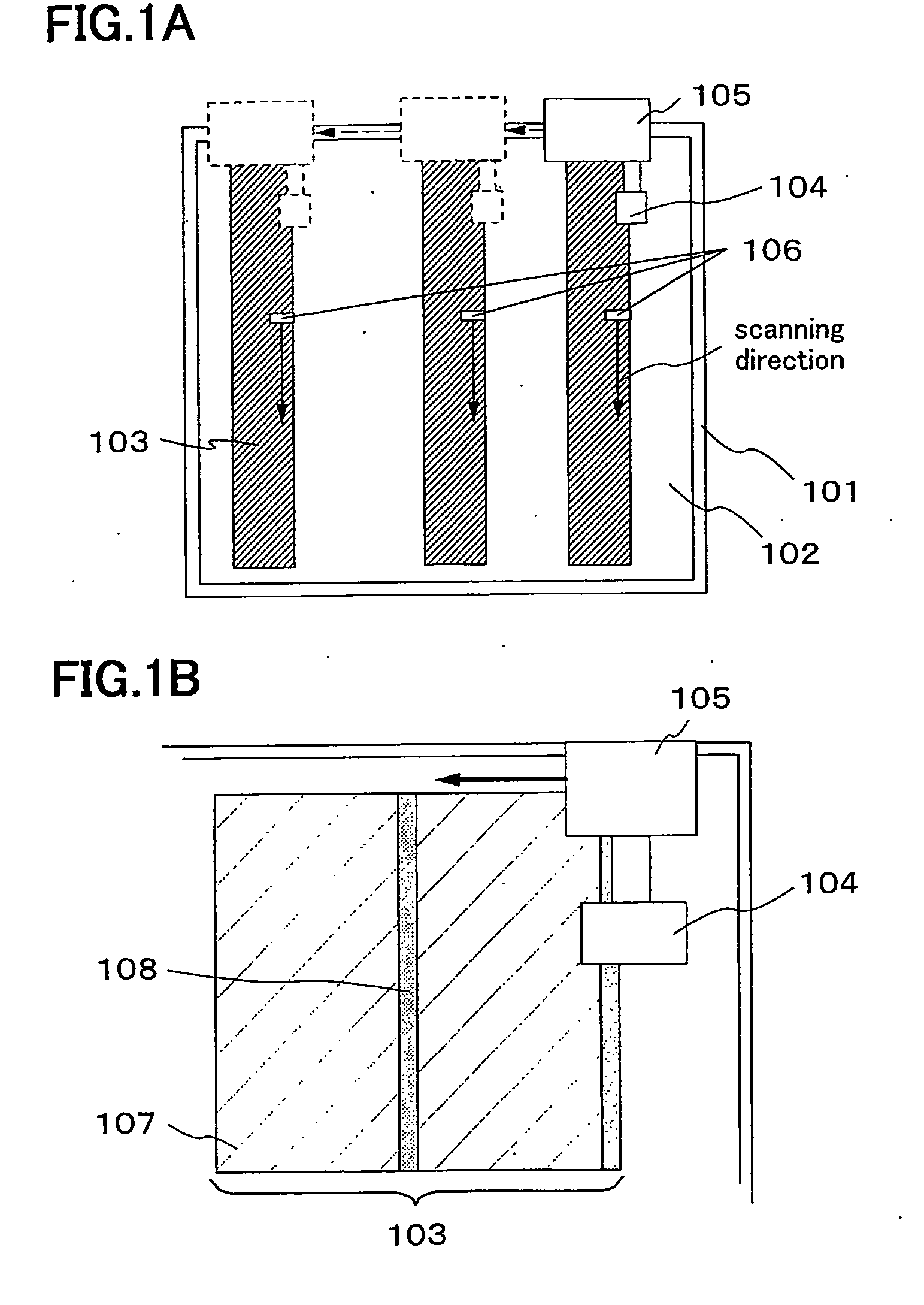
[0096]In this embodiment, an example of detecting a large grain size region and a poorly crystalline region by using laser which is separately provided is explained.

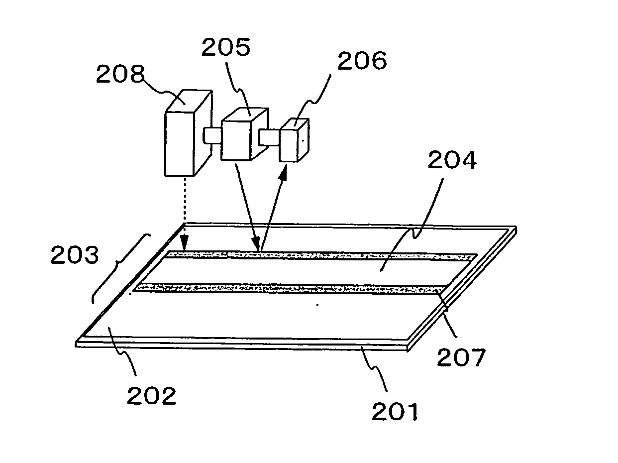
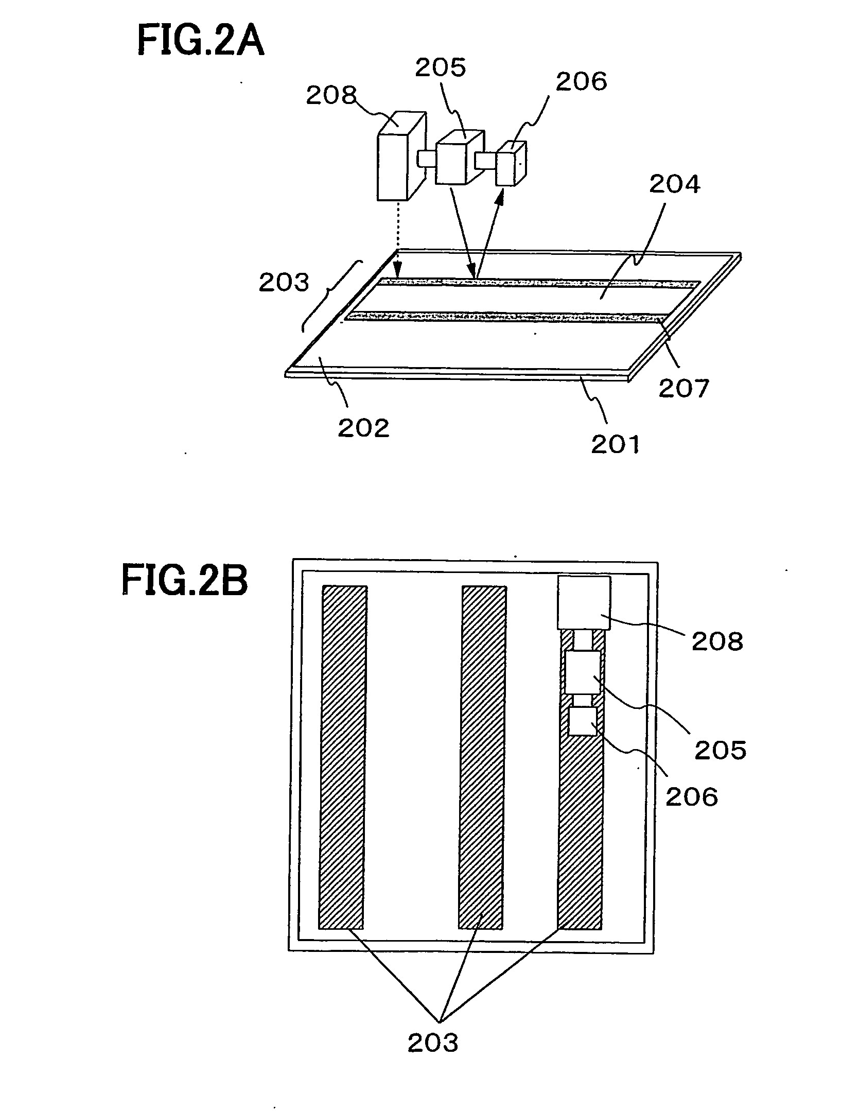
[0097]First, a non-single crystal semiconductor film 202 is formed over a substrate 201 in the same manner as in Embodiment Mode 1. Then, as shown in FIG. 2A, laser irradiation is conducted using the non-single crystal semiconductor film 202 as an irradiated surface to form a laser irradiation region 203.

[0098]Next, a resist is formed, and a large grain size region 204 in the laser irradiation region 203 is detected to determine a place where a photolithography step is conducted. In this embodiment, laser 205 and an optical sensor 206 are used. It is to be noted that the resist has only to be able to transmit the laser 205 to the degree that the large grain size region 204 and the poorly crystalline region 207 can be distinguished from each other.

[0099]The wavelength of the laser 205 is required to be able to detect the ...

embodiment 2

[0109]In this embodiment, a process of manufacturing a CMOS transistor using a p-channel TFT and an n-channel TFT manufactured by using the invention is explained with reference to drawings.

[0110]FIG. 8A shows a state just after laser irradiation is conducted with a plurality of laser irradiation apparatuses with respect to an amorphous semiconductor film 802 formed over a substrate 800. Hereinafter, a manufacturing process viewed from a cross section taken along a dotted line A-B in this drawing is explained.

[0111]As shown in FIG. 8B, a base film 801 is formed over a substrate 800 having an insulating surface. In this embodiment, a glass substrate is used as the substrate 800. As the substrate used here, a glass substrate formed of barium borosilicate glass, aluminoborosilicate glass, or the like, a quartz substrate, a ceramic substrate, a stainless steel substrate, or the like can be used. Moreover, although a substrate formed from synthetic resin typified by acrylic or plastic su...

embodiment 3

[0143]In this embodiment, a light emitting device using a light emitting element formed by using a TFT manufactured in another embodiment and an example of manufacturing the light emitting device are explained. The light emitting device which will be explained in this embodiment has a structure in which light is extracted from a substrate (hereinafter, referred to as opposing substrate) side which is opposed to a substrate having an insulating surface; however, the present invention is not limited to this structure and can be similarly used for a light emitting device having a structure in which light is extracted from a substrate side having an insulating surface, or a light emitting device having a structure in which light is extracted from both sides of a substrate side having an insulating surface and an opposing substrate side.

[0144]FIG. 12 is a top view of the light emitting device and FIG. 13 is a cross-sectional view taken along A-A′ of FIG. 12. Reference numeral 1200 denote...


PUM

PropertyMeasurementUnit
Grain sizeaaaaaaaaaa
Timeaaaaaaaaaa
Concentrationaaaaaaaaaa

Abstract

When annealing of a semiconductor film is conducted using a plurality of lasers, each of the distances between laser irradiation regions is different. When a lithography step is conducted in accordance with a marker which is formed over a substrate in advance after the step, light-exposure is not correctly conducted to a portion crystallized by laser. By using a laser irradiation region obtained on a laser irradiation step as a marker, light-exposure is conducted by making a light-exposure position of a stepper coincide with a large grain size region in the laser irradiation region. A large grain size region and a poorly crystalline region are detected by utilizing a thing that scattering intensity of light is different between the large grain size region and the poorly crystalline region, thereby determining a light-exposure position.

Description

TECHNICAL FIELD[0001]The present invention relates to a method for conducting light-exposure treatment precisely to a region in which a crystal with a large grain size is formed by a laser crystallization step in a photolithography step after the laser crystallization step and a light-exposure apparatus of conducting a step of this treatment. Moreover, the invention relates to a semiconductor device manufactured by conducting this treatment and a manufacturing method thereof.BACKGROUND ART[0002]Nowadays, technique for manufacturing a thin film transistor (hereinafter, referred to as a TFT) over a substrate is drastically progressing, and the application and development thereof to an active matrix display device are being advanced. In particular, a TFT using a polycrystalline semiconductor film has higher electron field-effect mobility (also referred to as mobility) than that of a TFT using a conventional non-single crystal semiconductor film; therefore, high speed operation can be c...

Claims


Application Information

Patent Timeline
IPC IPC(8): G01B11/30H01L21/027
CPCG03F7/70383H01L21/2026Y10T29/41H01L27/1266H01L27/1285H01L21/268H01L21/02686H01L21/0242H01L21/02683H01L21/02691H01L21/02425H01L21/02488H01L21/02422H01L21/02532H01L21/02678H01L21/02675
Inventor TANAKA, KOICHIROYAMAMOTO, YOSHIAKI
Owner SEMICON ENERGY LAB CO LTD
Why Eureka
Try Eureka