Nanopore arrays and sequencing devices and methods thereof

Inactive Publication Date: 2008-10-16
TRUSTEES OF BOSTON UNIV
View PDF11 Cites 121 Cited by
  • Summary
  • Abstract
  • Description
  • Claims
  • Application Information

AI Technical Summary

Benefits of technology

[0023]The present invention further provides a method, comprising: inducing linear passage of at least a portion of a molecule through at least a portion of 100 or more nanopores, wherein each nanopore comprises at least one inner surface, wherein each nanopore has a characteristic cross-sectional dimension i

Problems solved by technology

These natural nanopores, however, have certain drawbacks as pertains to characterizing DNA and other macromolecules.
Such natural nanopores are mechanically and chemically instable, and, in some cases, are toxic.
In addition, devices using α-hemolysin nanopores to sequence DNA and RNA molecules, have, to date, failed to read the sequence of the molecules at a single-nucleotide resolution; only stretches of tens of bases of the same nucleotide can be distinguished from each other, such as poly adenosine (poly A) from poly cytosine (poly C), and poly A from poly deoxyadenosine (poly dA), by the difference in the ionic current blockade as well as the speed at which the polymer passes the nanopores.
It is known that in existing techniques, individual nucleotides or base-pairs pass through the nanopore too quickly to allow an accurate determination of the blockage current.
While the fabrication of nanometer-sized pores on solid state materials is p

Method used


Image

  • Nanopore arrays and sequencing devices and methods thereof
  • Nanopore arrays and sequencing devices and methods thereof
  • Nanopore arrays and sequencing devices and methods thereof

Examples


example 1

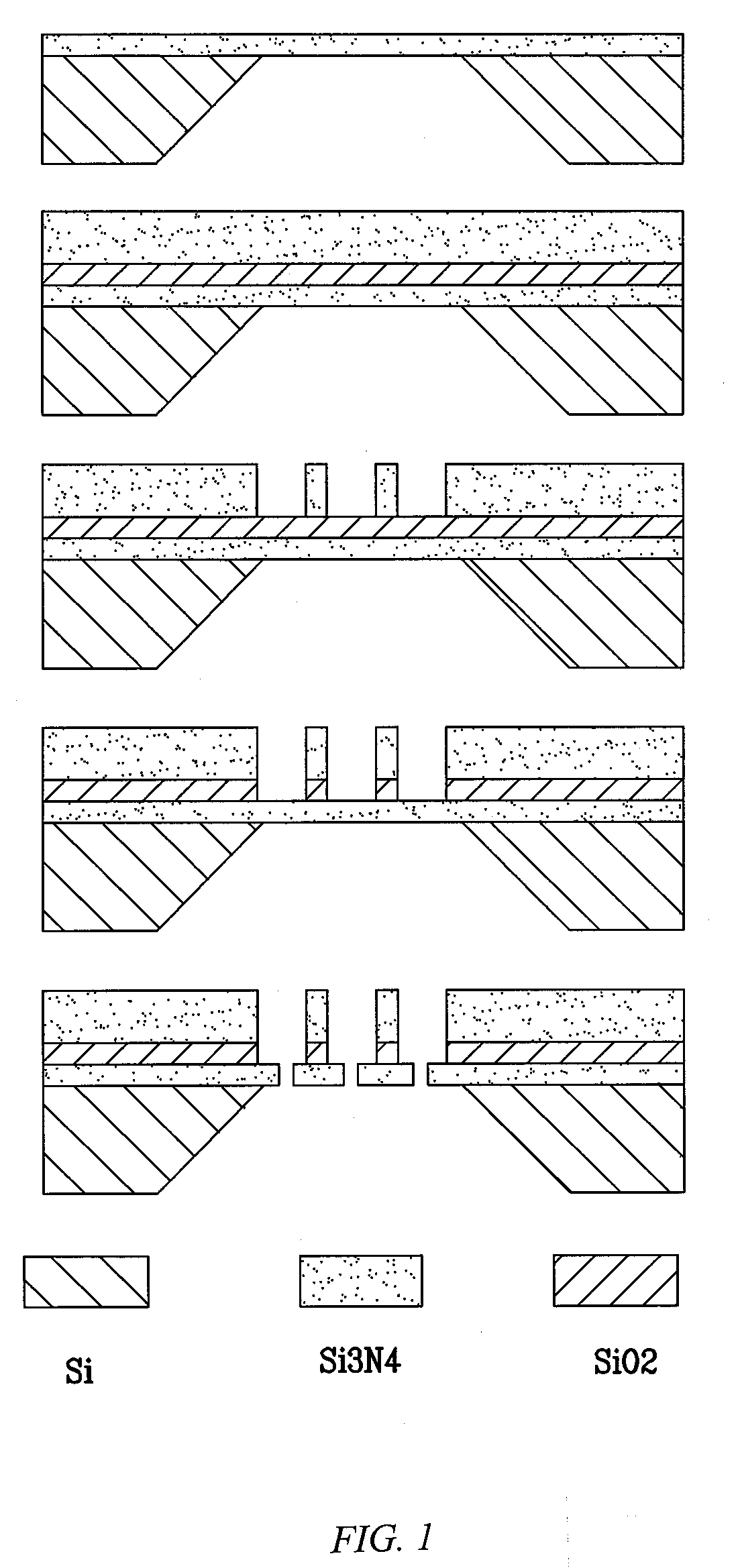
[0100]Solid-state nanopores were fabricated; all fabrications started with formation of a 50 nm thick DuraSiN™ silicon nitride membrane (Protochips Inc, Raleigh, N.C.). Solid-state nanopores were directly drilled by a JEOL 2010F field emission TEM.

[0101]Alignment of the electron probe involved condenser stigmation to the familiar triangle shaped beam, using a large condenser aperture; the probe seen is dominated by three-fold aberrations. The condenser lens was fully converged to crossover then slightly over focused. The resultant beam was an intense point with a triangular halo of low intensity. The remainder of the column alignment followed from normal high resolution transmission electron microscopy (“HRTEM”) alignment procedures. After the alignment of the electron probe, nanopores with characteristic cross-sectional dimensions in a range of 3-6 nm were directly drilled by an electron beam intensity of about 2.5×10⁸ e / nm2s using a magnification of 800 K. The time for pore format...

example 2

[0103]A two-layer structure, 200 nm of SiO2 and 500 nm thick capping layer of Si3N4, was formed by plasma enhanced chemical vapor deposition (PECVD). A focused ion beam (FIB) drilled a 2 micrometer characteristic cross-sectional dimension well array in the first 500 nm thick silicon nitride layer. After this process, the silicon dioxide layer was removed by buffered oxide etch (BOE), to a 50 nm thick silicon nitride membrane for single nanometer scale pores.

[0104]An array of low-density nanopores (2×2, 3×3, and 6×6) was integrated into a monolithic silicon-based chip using scanning transmission electron microscope (STEM). The arrays were formed by patterning beam scanning without well arrays. Automated patterning of nanopores was accomplished by operating the microscope in STEM mode and directly addressing the scan coils to deflect the beam by the desired amount. This method was enabled by direct beam control through either an analytical x-ray acquisition system or dedicated electro...

example 3

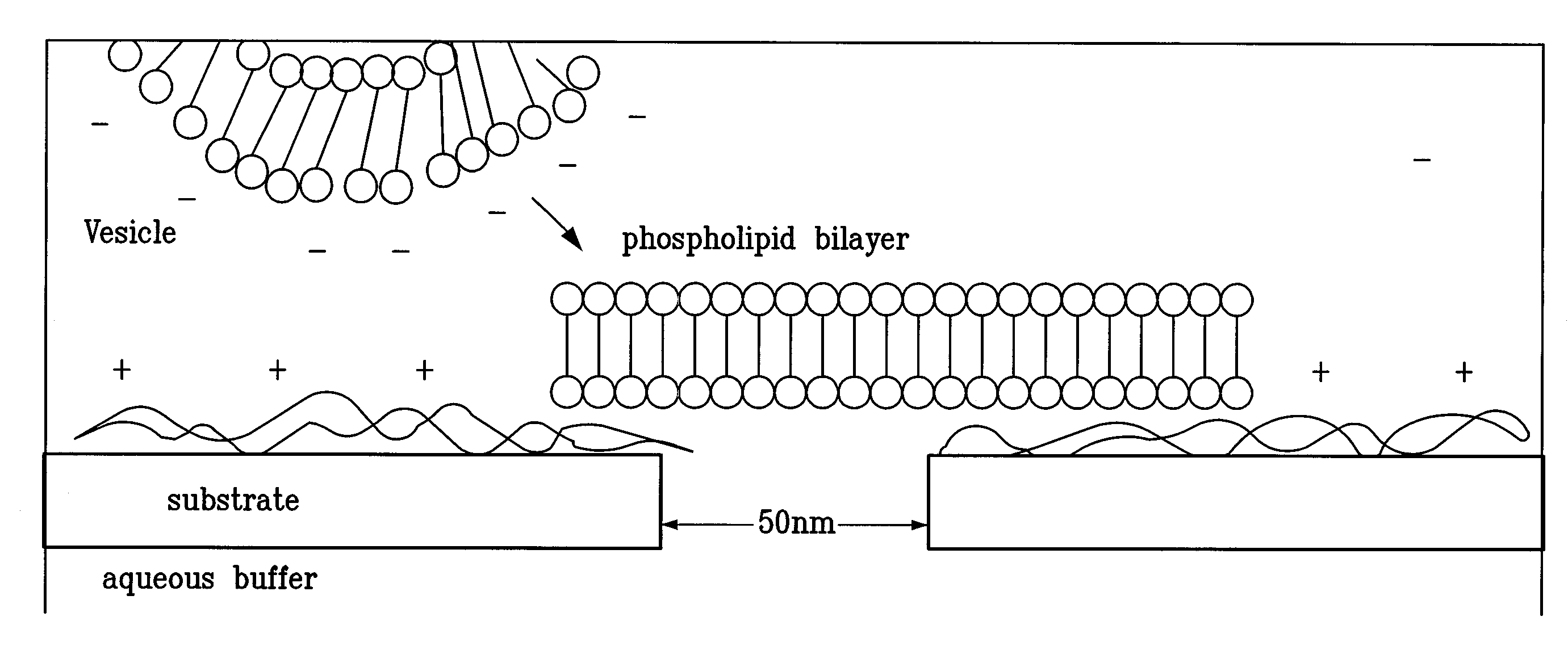
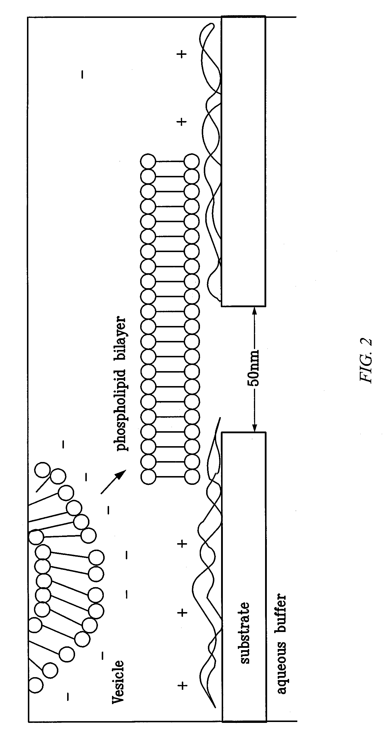
[0105]FIG. 5 illustrates a comparison between the proteinaceous α-HL nanopore and a drawing of a chemically modified solid-state nanopore. In principle, both the thickness of the coating and the terminal group can be controlled, rendering this approach highly versatile. The coated nanopores are directly imaged.

[0106]Nanopores were characterized using ellipsometry, atomic force microscopy (AFM), and X-ray photoelectron spectroscopy (XPS) on model substrates, consisting of 50-nm-thick Si3N4 films evaporated by LPCVD on Si wafers.

[0107]Following drilling of the nanopores by TEM, the chips were placed in a 10×75 mm test tube and about 3 ml fresh solution of boiling piranha was added (4:7 30% H2O2: 98% H2SO4). The beaker was heated to sustain boiling for 15 min, after which the piranha solution was removed and the chip was thoroughly rinsed with Millipore water, methanol, and dried using N2 stream. The chips remained hydrophilic in ambient air for less than about 10 minutes.

[0108]Three t...


PUM

PropertyMeasurementUnit
Lengthaaaaaaaaaa
Thicknessaaaaaaaaaa
Thicknessaaaaaaaaaa

Abstract

Provided are devices comprising one or more nanoscale pores for use in, inter alia, analyzing various biological molecules. Also provided are methods for the fabrication of nanoscale pores in solid-state substrates, methods for functionalizing nanopores in solid-state substrates, and methods for sequencing polymers using devices containing nanoscale pores.

Description

CROSS-REFERENCE TO RELATED APPLICATIONS[0001]This application claims the benefit of U.S. Provisional Application No. 60 / 891,759 filed Feb. 27, 2007, the entirety of which is incorporated by reference herein.FIELD OF THE INVENTION[0002]The present invention pertains to the field of structures having nanoscale pores. The present invention also pertains to the field of fabrication of nanoscale devices.BACKGROUND OF THE INVENTION[0003]Various scientific and patent publications are referred to herein. Each is incorporated by reference in its entirety.[0004]The rapid determination of the nucleotide sequence of single- and double-stranded DNA and RNA is a major goal of researchers seeking to obtain the sequence for the entire genome of an organism. The ability to determine the sequence of nucleic acids in DNA or RNA has additional importance in identifying genetic mutations and polymorphisms.[0005]The concept of using nanometer-sized holes, or “nanopores,” to characterize biological macrom...

Claims


Application Information

Patent Timeline
IPC IPC(8): C40B20/04C40B60/00C40B50/18B23K15/00C40B30/00
CPCB82Y30/00G01N33/48721
Inventor KIM, MINJUNMULERO, RAFAELSTEAGER, EDWARD
Owner TRUSTEES OF BOSTON UNIV
Why Eureka
Try Eureka