Method of producing compound nanorods and thin films

a technology of compound nanomaterials and thin films, applied in the direction of polycrystalline material growth, nuclear engineering, transportation and packaging, etc., can solve the problems of micron scale liquid droplets, undesirable inhomogeneity of deposition, and inevitably evaporated target surface materials, etc., and achieve high laser fluence and high laser fluence

Inactive Publication Date: 2008-11-27
IMRA AMERICA
View PDF8 Cites 16 Cited by
  • Summary
  • Abstract
  • Description
  • Claims
  • Application Information

AI Technical Summary

Benefits of technology

[0011]A slight variation of the above method can switch the growth mode to 2D thin film growth. This is realized by using the same high laser fluence throughout both growth steps. In practice, for many film / substrate systems that have large lattice mismatch between the film and substrate (e.g., ZnO / sapphire), while maintaining the same high laser fluence that can fully vaporize the source material, the first step will be performed at a low substrate temperature, providing a buffer layer. At the second step, the substrate temperature can be raised to grow the main layer. In this way, a 2D growth mode can be achieved.

Problems solved by technology

Regarding the VLS method that is commonly used for growth of nanorods and nanowires, because the pre-deposited metal catalyst can bring in an undesirable impurity for many applications (for example, gold is detrimental to silicon devices), many attempts have been tried to develop non-catalytic or self-catalytic (i.e., using the same material intended for growth as the catalyst) growth methods.
Under such intense laser irradiation, the target surface material is inevitably evaporated.
One drawback of high power nanosecond PLD is the generation of micron scale liquid droplets, which is mainly a result of liquid splashing and collateral damage of the target near the focal spot due to the high pulse energy.
These large droplets introduce undesirable inhomogeneity to the deposition, especially in thin film growth.
First, the extremely short pulse duration means a much higher peak power.

Method used


Image

  • Method of producing compound nanorods and thin films
  • Method of producing compound nanorods and thin films
  • Method of producing compound nanorods and thin films

Examples


Embodiment Construction

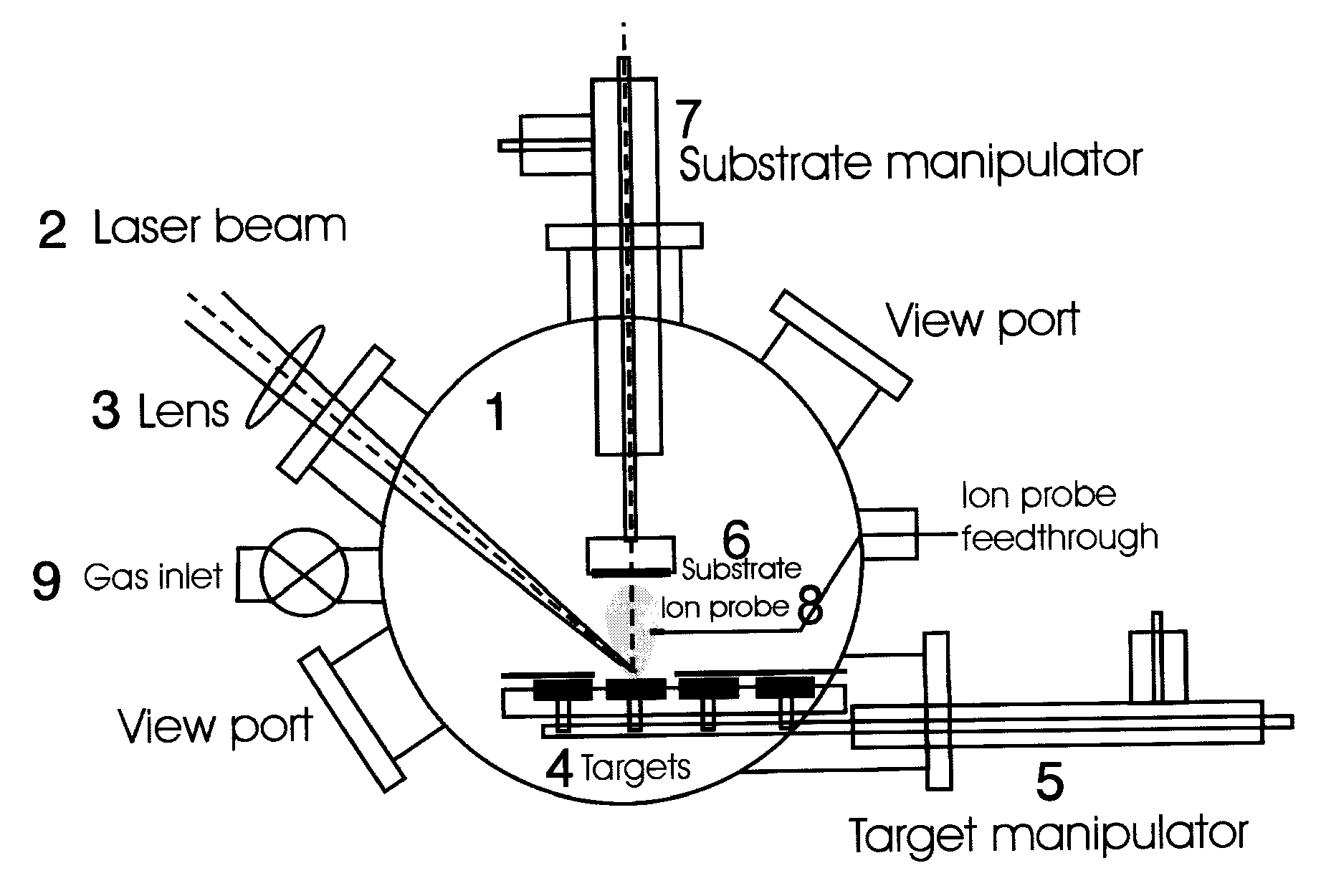
[0025]FIG. 1 illustrates the experimental setup of ultrafast pulsed laser ablation used in this invention. The system basically includes a vacuum chamber for deposition (base pressure 1×10⁻⁶ Torr) and an ultrafast pulsed laser for ablation. The chamber contains a target manipulator, a substrate manipulator, and an ion probe. Four disk-like targets can be mounted on the target manipulator. During ablation, the targets rotate and move laterally (i.e., in the target surface plane) back and forth. To improve deposition uniformity, the substrate can also rotate and move in its surface plane. The substrate heater can supply a temperature up to 1000° C. The laser used in the experiments has a pulse duration of 500 fs, a central wavelength of 1.03 μm, a pulse energy up to 100 μJ, and a repetition rate up to several hundreds of kHz. The laser is focused using a lens onto the target surface through a fused silica window. During ablation, a biased charge probe can be inserted in front of the p...


PUM

PropertyMeasurementUnit
temperatureaaaaaaaaaa

Abstract

A method of producing compound nanorods and thin films under a controlled growth mode is described. The method involves ablating compound targets using an ultrafast pulsed laser and depositing the ablated materials onto a substrate. When producing compound nanorods, external catalysts such as pre-deposited metal nanoparticles are not involved. Instead, at the beginning of deposition, simply by varying the fluence at the focal spot on the target, a self-formed seed layer can be introduced for nanorods growth. This provides a simple method of producing high purity nanorods and controlling the growth mode. Three growth modes are covered by the present invention, including nanorod growth, thin film growth, and nano-porous film growth.

Description

FIELD OF INVENTION[0001]This invention relates to growth of compound nanomaterials and thin films using ultrafast pulsed laser ablation and deposition.BACKGROUND OF THE INVENTION[0002]Nanomaterials have important potential applications in modern technologies. Depending on the number of spatial dimensions on which the material expands beyond the nanoscale, nanomaterial can be classified as zero-dimensional (nanoparticles), one-dimensional (nanorods and nanowires), and two-dimensional (nanosheets and nanometer thin films). For each of these categories of nanomaterials, the synthesis methods are different. For example, nanoparticles are often produced using the sol-gel process; nanorods are often produced using the vapor-liquid-solid (VLS) process [S. Wagner and W. C. Ellis, Applied Physics Letters, Vol. 4 (1964), 89; A. M. Morales and C. M. Lieber, Science, Vol. 279 (1998), 208; W. Lu, C. M. Lieber, Journal of Physics D: Applied Physics, Vol 39 (2006), R387, S. C. Tjong ed., Nanocryst...

Claims


Application Information

Patent Timeline
Patent Type & Authority Applications(United States)
IPC IPC(8): B05D3/12
CPCC23C14/086C23C14/28Y10T428/25C30B29/16C30B29/60C30B23/00
Inventor LIU, BINGHU, ZHENDONGCHE, YONG
Owner IMRA AMERICA
Why Eureka
Try Eureka