Compared to the rest of the EM spectrum, X- and gamma-rays can cause particularly severe, long term damage to various types of matter found in
solid structures.
Comparatively
high potential for damage occurs from
exposure to external gamma radiation because gamma photons have higher energy per
photon, thus high frequencies, short wavelengths and tremendous penetrating power compared to charged particles such as alphas and betas (energetic electrons).
The size of these currents can be orders of magnitude greater than normal
system levels and can cause temporary or permanent damage to electronic circuits, depending on specific circumstances.
Both
CMOS devices and
MOSFET transistors are affected by photocurrents; free charge can be permanently trapped in certain
oxide materials.
However, depending on the size of the transient, this effect can also lead to permanent changes if there is actual junction burn-out or a “latch up”.“Latchup”—is a particularly destructive
ionization effect that can potentially lead to
catastrophic failure of electronic devices.
Such an unnatural flow of current within a highly ordered device can cause a circuit to temporarily malfunction—in the worst case, a tiny segment of the device can be physically burned-out through
joule heating of the material.
Such displacements can cause permanent physical changes in lattice structure (e.g. various types of structural defects) and drastically alter the properties of materials (e.g. changes in bandgap energy levels), depending upon the total “
dose” and
dose rate of gamma photons as well as the precise locations of resulting
lattice defects.
“Rad hard” integrated circuits and
electronic systems for military and space applications are substantially more expensive than ordinary commercial products.
Many of the essential features of this unique market segment are summarized in quotes from an employee of a company, Maxwell Technologies that is well known for its product lines of rad hard components and systems:“The trouble is, building “hardened by design”
electronics takes years, the costs are high, and at the end, the systems are often out of date with the current commercial state-of-the-art.
Electrons and protons can be shielded against relatively effectively, while energetic heavy ions and gamma radiation are difficult to shield against.
Simple slab shields are rather effective in dealing with omni-directional
space radiation but are insufficient against X-rays [and especially even higher energy gamma rays].
This includes thousands of low-level unintended releases, as well as the major disaster at the Chernobyl reactor complex in Russia in 1986.
Also, a variety radioisotopes produced in nuclear reactors (e.g. 60Co) began to be used commercially as radiation sources in many industrial and medical applications, creating additional
human exposure and used equipment disposal issues.
However, by contrast,
nuclear reaction rates in commercial reactors are tightly controlled, and thus produce a more-or-less continuous flux of gamma radiation, unlike the time-compressed, very intense bursts associated with nuclear weapons.
Since size or weight does not particularly matter in commercial nuclear reactors, shielding against various types of radiation, including gammas, can be massive and extensive.
However, delayed gamma radiation emanating from radioisotopes found in spent reactor fuel rods presents a more problematic safety issue than nuclear reactors themselves, since the rods must be physically removed from heavily shielded reactors after their use.
Two key technological problems that must be solved to harness the potential power of nuclear isomers for both weapons and
energy storage applications are: (a) triggering them efficiently in a manner that permits a
net energy gain from the point of triggering through decay; and (b) triggering enormous numbers of isomer atoms to decay in
unison at exactly the same time.
For
energy storage applications there is also a third major problem: efficiently absorbing and converting gamma radiation into some other form of energy that can be more readily utilized to do work.
DOE convened a scientific panel to determine whether 178mHf production was feasible; the panel answered yes, but at very high cost.
To date, none of these problems have been solved.
With the foregoing hypothetical
aerospace applications, assuming that net-
gain isomer triggering can be made to work, there is one additional major technological issue: low-
mass materials that can provide critical, “
mass-effective” shielding against gamma radiation.
However, their work has not been replicated by others and, in the opinion of some scientists, has been totally discredited.
The greatest danger from the vast majority of alpha and beta particles is not created by external
exposure to them (since shielding against them is almost trivial), but rather when they are somehow transported or produced inside a living
organism or a nonliving physical
enclosure containing sensitive electronic components.
Unfortunately, many types of materials can be “activated” by
neutron absorption and subsequently produce prompt or delayed gammas and radioactive isotopes as a result; thus, gamma shielding may also be required.
Neutrons are particularly damaging to living organisms because of their being composed of a high percentage of
hydrogen (˜60%) associated with carbon-
hydrogen bonds in biological molecules.
Being
electromagnetic radiation, gamma photons are attenuated exponentially; thus, it is not theoretically possible to design a shield that will stop 100% of all incident gamma radiation.
As a result, gamma rays and hard X-rays are much more difficult to attenuate or shield against than
charged particle radiation such as alphas or betas.
Also, as
gamma photon energies get higher, they are somewhat more difficult to attenuate; a 5 MeV
gamma photon has more penetrating power than a 1 MeV gamma
photon.
Although the U.S. military would willingly pay for the high cost of gamma shielding, existing high performance shielding materials cannot provide an effective shield with a
mass that is low enough for both gamma attenuation and combat aircraft performance requirements to be met.
Since DU and
thorium are both slightly radioactive, their use may be barred in certain commercial shielding applications because of environmental and
human health safety issues.
At this time, lead is hard to surpass for cost-effectiveness in appropriate gamma shielding applications.
Shielding for such
neutron-rich nuclear environments can potentially be more difficult because (depending upon the
isotopic composition of the neutron absorbers)
neutron capture events frequently result in the production of prompt gammas, which tend to have higher average
photon energies than delayed gammas produced in common nuclear decay chains (in which
excess energy, Q, can often be distributed across a greater number of reaction products over a longer period of time).


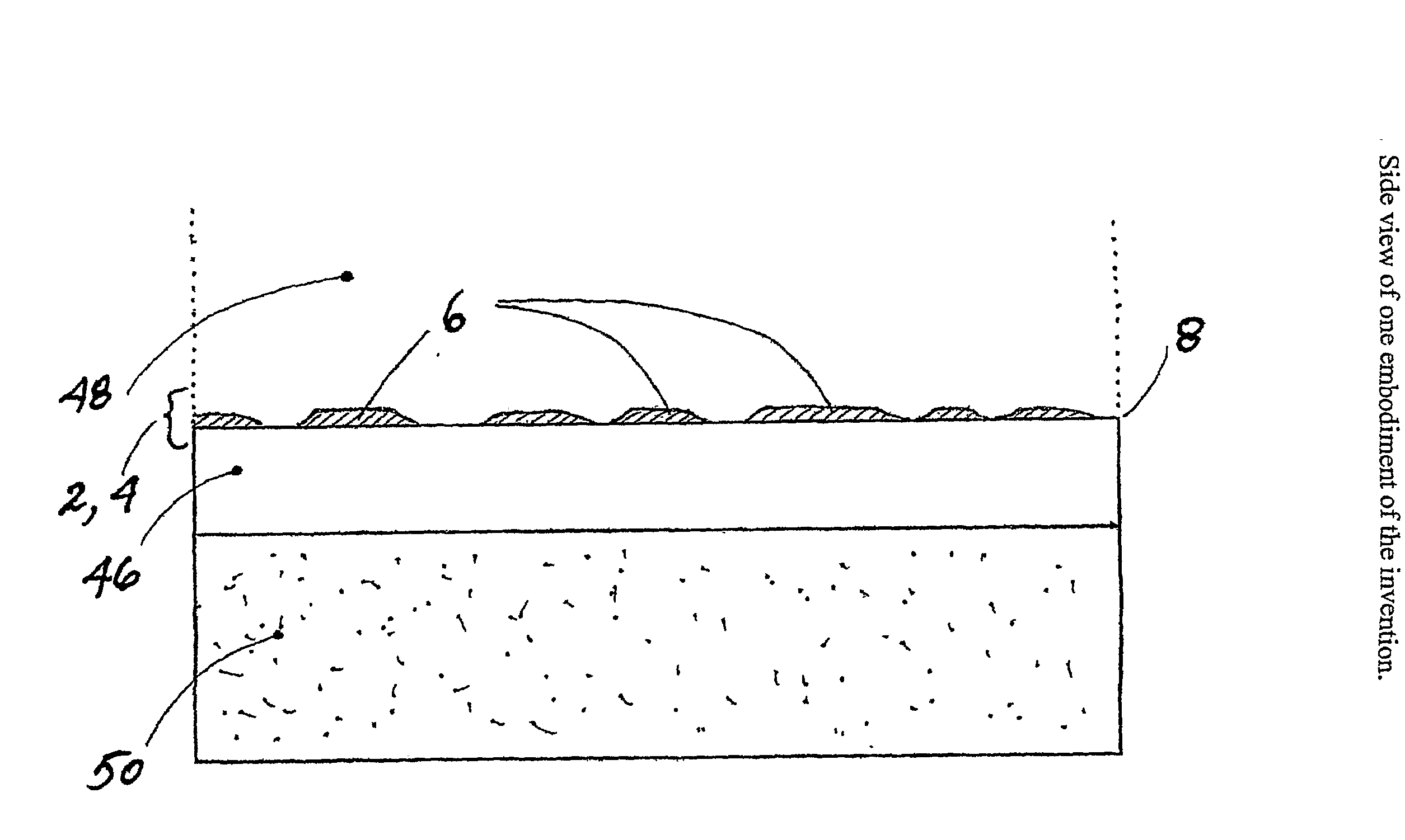