Silicon Nanocrystal Embedded Silicon Oxide Electroluminescence Device with a Mid-Bandgap Transition Layer

a silicon oxide and silicon nanocrystal technology, applied in the direction of coatings, metallic material coating processes, chemical vapor deposition coatings, etc., can solve the problems of low ion/neutral ratio, low ion/neutral ratio, low turn-on voltage, and low ion/neutral ratio, etc., to achieve low turn-on voltage, low tunneling efficiency, and high ion/neutral ratio

Active Publication Date: 2008-12-11
SHARP KK
View PDF6 Cites 1 Cited by
  • Summary
  • Abstract
  • Description
  • Claims
  • Application Information

AI Technical Summary

Benefits of technology

[0021]A method is provided to achieve low turn-on voltages for electrically pumped Si nanocrystal embedded oxide (SiOx) light emitting devices (LEDs). The active layers of the LEDs are SiOx deposited on Si wafers using HDPCVD (high density plasma-enhanced chemical vapor depositions) processes. The carrier transport process inside the LEDs is Fowler-Neidheim tunneling. Since the barrier height of SiOx is high, the tunneling efficiencies are low. However, a SiNx layer, or similar material, having a smaller barrier height, can be introduced between the SiOx layer and Si wa

Problems solved by technology

However, the indirect band-gap makes it an inefficient material for light emitting optoelectronic devices.
However, conventional PECVD and sputtering techniques have the limitations of low plasma density, inefficient power coupling to the plasma, low ion/neutral ratio, and uncontrolled bulk, and interface damage due to high ion bombardment energy.
Therefore, the oxide films formed from a conventional capacitively-coupled plasma (CCP) generated plasma may create reliability issues due to the high bombardment energy of the impinging ionic species.
However, it is not possible to control the ion energy using radio frequency (RF) of CCP generated plasma.
Any attempt to enhance the reaction kinetics by increasing the applied power results in increased bombardment of the deposited film, which creates a poor quality films with a high defect concentration.
Additionally, the low plasma density associated with these types of sources (˜1×10⁸-109 cm−3) leads to limited reaction possibilities in the plasma and on the film surface, inefficient

Method used


Image

  • Silicon Nanocrystal Embedded Silicon Oxide Electroluminescence Device with a Mid-Bandgap Transition Layer
  • Silicon Nanocrystal Embedded Silicon Oxide Electroluminescence Device with a Mid-Bandgap Transition Layer
  • Silicon Nanocrystal Embedded Silicon Oxide Electroluminescence Device with a Mid-Bandgap Transition Layer

Examples


Embodiment Construction

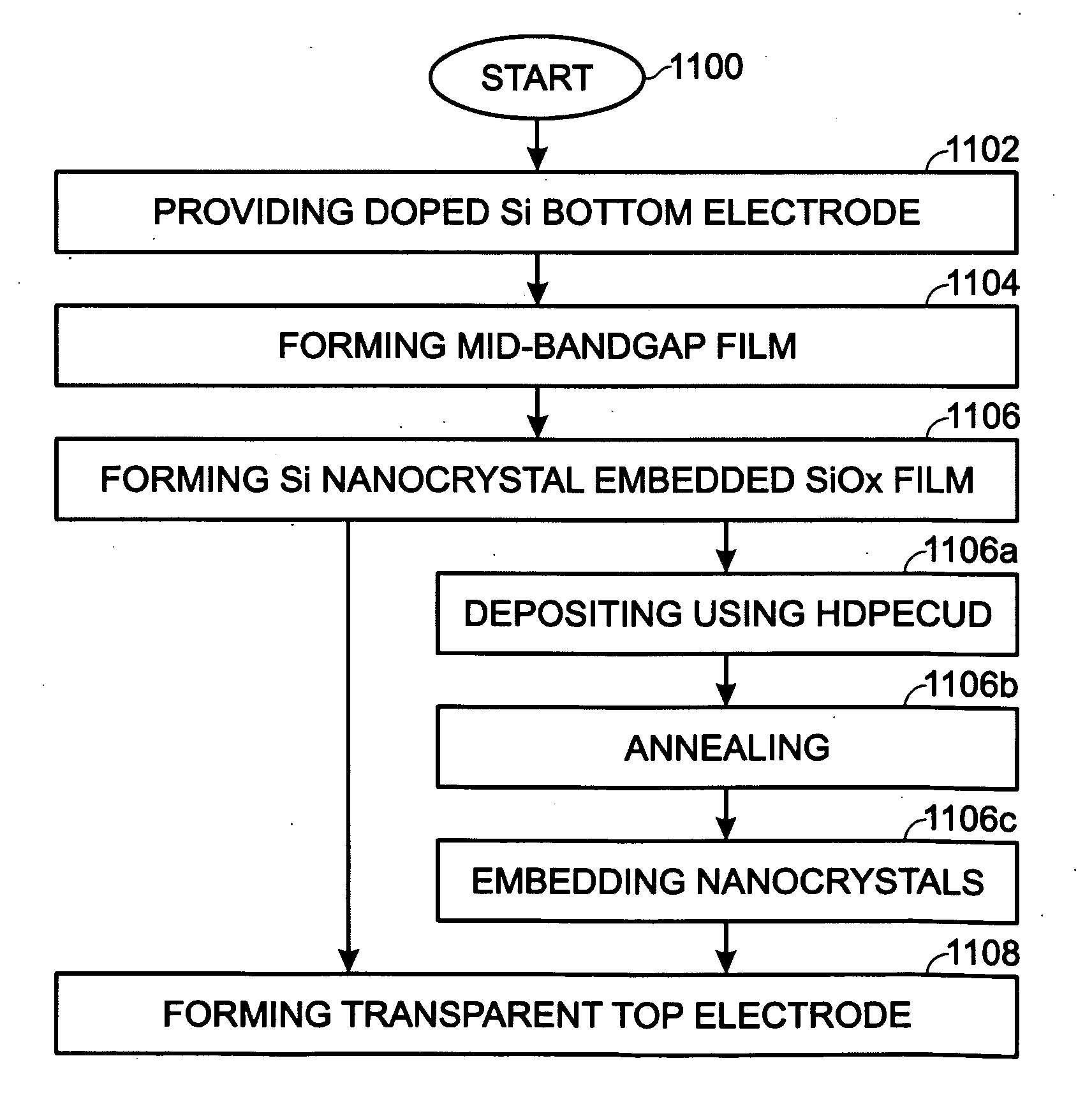
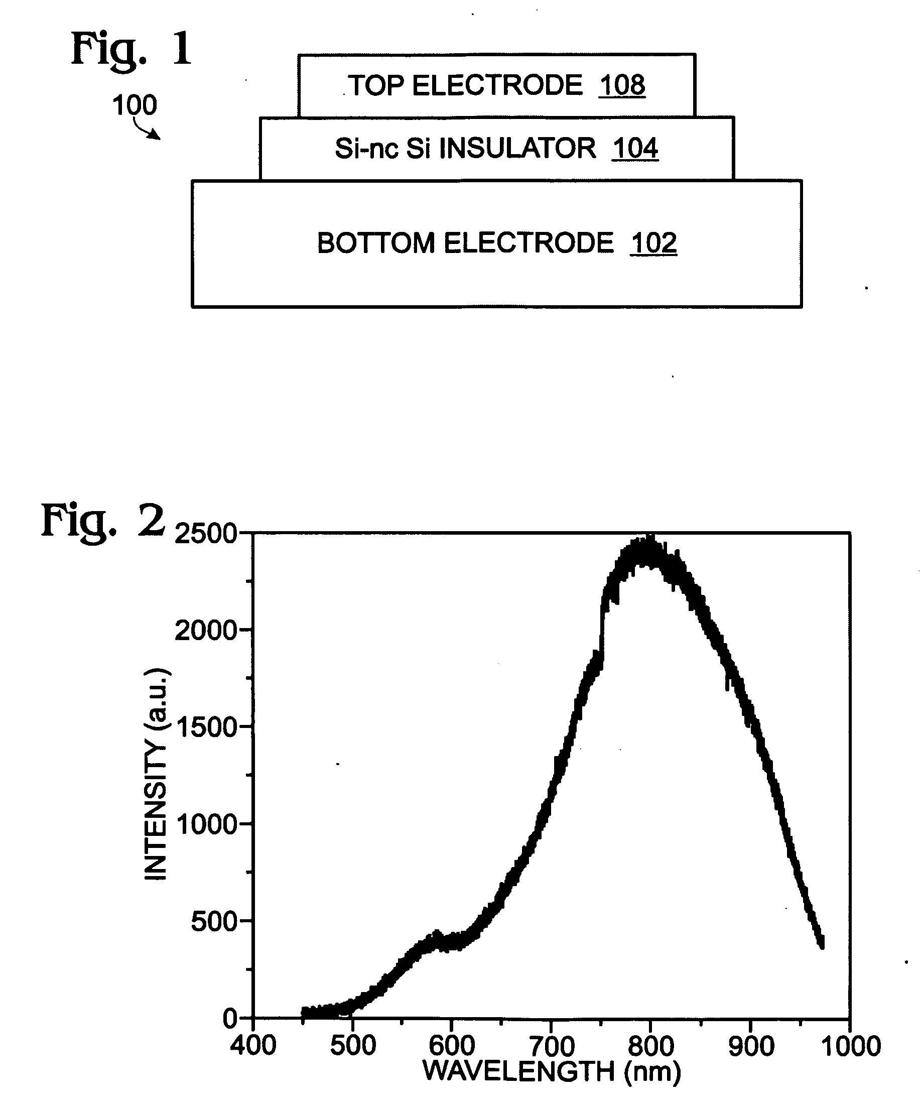
[0038]FIG. 1 is a partial cross-sectional view of an electroluminescence (EL) device made using a silicon (Si) nanocrystal embedded silicon oxide (SiOx) film. The electrically pumped light emitting device 100 is fabricated using a Si nanocrystal embedded SiOx film 104 as active layer overlying a doped silicon wafer 102. A transparent top electrode 108 of ITO (Indium Tin Oxide) overlies the SiOx film 104. The SiOx active layer 104 can be deposited using HDPCVD (High Density Plasma-enhanced Chemical Vapor Depositions) processes, as explained in more detail below.

[0039]FIG. 2 is a graph depicting the light intensity of an exemplary SiOx EL device as a function of wavelength. The surface emission wavelength is centered around 800 nm with a spectral width of about 150 nm (Full Width at Half Magnitude). A monochromator with a multiple-mode fiber may be used as a probe to collect and deliver light from an EL device and to measure the light emitting spectra. An emissions peak at ˜800 nanome...


PUM

PropertyMeasurementUnit
Temperatureaaaaaaaaaa
Thicknessaaaaaaaaaa
Thicknessaaaaaaaaaa

Abstract

A method is provided for forming a silicon (Si) nanocrystal embedded Si oxide electroluminescence (EL) device with a mid-bandgap transition layer. The method provides a highly doped Si bottom electrode, and forms a mid-bandgap electrically insulating dielectric film overlying the electrode. A Si nanocrystal embedded SiOx film layer is formed overlying the mid-bandgap electrically insulating dielectric film, where X is less than 2, and a transparent top electrode overlies the Si nanocrystal embedded SiOx film layer. The bandgap of the mid-bandgap dielectric film is about half that of the bandgap of the Si nanocrystal embedded SiOx film. In one aspect, the Si nanocrystal embedded SiOx film has a bandgap (Eg) of about 10 electronvolts (eV) and mid-bandgap electrically insulating dielectric film has a bandgap of about 5 eV. By dividing the high-energy tunneling processes into two lower energy tunneling steps, potential damage due to high power hot electrons is reduced.

Description

RELATED APPLICATIONS[0001]This application is a continuation-in-part of a pending patent application entitled, LIGHT EMITTING DEVICE WITH A NANOCRYSTALLINE SILICON EMBEDDED INSULATOR FILM, invented by Huang et al., Ser. No. 12 / 126,430, filed on May 23, 2008, Attorney Docket No. SLA2270, which is a Continuation-in-Part of the following applications:[0002]SILICON OXIDE THIN-FILMS WITH EMBEDDED NANOCRYSTALLINE SILICON, invented by Pooran Joshi et al., Ser. No. 11 / 418,273, Attorney Docket No. SLA0963, filed May 4, 2006;[0003]ENHANCED THIN-FILM OXIDATION PROCESS, invented by Pooran Joshi et al., Ser. No. 11 / 327,612, Attorney Docket No. SLA8012, filed Jan. 6, 2006;[0004]HIGH-DENSITY PLASMA HYDROGENATION, invented by Pooran Joshi et al., Ser. No. 11 / 013,605, filed Dec. 15, 2004;[0005]DEPOSITION OXIDE WITH IMPROVED OXYGEN BONDING, invented by Pooran Joshi, Ser. No. 10 / 801,377, filed Mar. 15, 2004;[0006]HIGH-DENSITY PLASMA OXIDATION FOR ENHANCED GATE OXIDE PERFORMANCE, invented by Joshi et a...

Claims


Application Information

Patent Timeline
IPC IPC(8): H01L21/00
CPCC23C16/24C23C16/30C23C16/401C23C16/505C23C16/56H01L21/02164H01L21/0217H01L21/02274H01L21/02532H01L21/02601H01L21/0262H01L21/31608
Inventor HUANG, JIANDONGJOSHI, POORAN CHANDRAZHANG, HAOVOUTSAS, APOSTOLOS T.
Owner SHARP KK
Why Eureka
Try Eureka