
Pattern forming method, resist composition to be used in the pattern forming method, negative developing solution to be used in the pattern forming method and rinsing solution for negative development to be used in the pattern forming method

a technology of resist composition and pattern forming method, which is applied in the direction of photomechanical equipment, instruments, photosensitive materials, etc., can solve the problems of reducing optical contrast, unable to achieve sufficient focal depth, and unable to establish sufficient resolution performance, etc., to achieve high degree of integration, high precision and fine pattern, and stable form

Active Publication Date: 2009-01-08
FUJIFILM CORP
View PDF82 Cites 75 Cited by
  • Summary
  • Abstract
  • Description
  • Claims
  • Application Information

AI Technical Summary

Benefits of technology

[0026]To solve the above-described problem and stably form a highly precise and fine pattern to thereby produce a highly integrated and highly precise electronic device, the present invention aims at providing a pattern forming method whereby line edge roughness can be relieved and the dimensional stability of the pattern can be improved.
[0028](a) coating a substrate with a resist composition comprising a resin that comprises a repeating unit represented by a following general formula (NGH-1), and, by the action of an acid, increases the polarity and decreases the solubility in a negative developing solution;
[0037](A) a resin that comprises a repeating unit represented by a following general formula (NGH-1), and, by the action of an acid, increases the polarity and decreases the solubility in a negative developing solution;
[0043](A) a resin that comprises a repeating unit represented by a following general formula (NGH-1), and, by the action of an acid, increases the polarity, decreases the solubility in a negative developing solution and increases the solubility in a positive developing solution;

Problems solved by technology

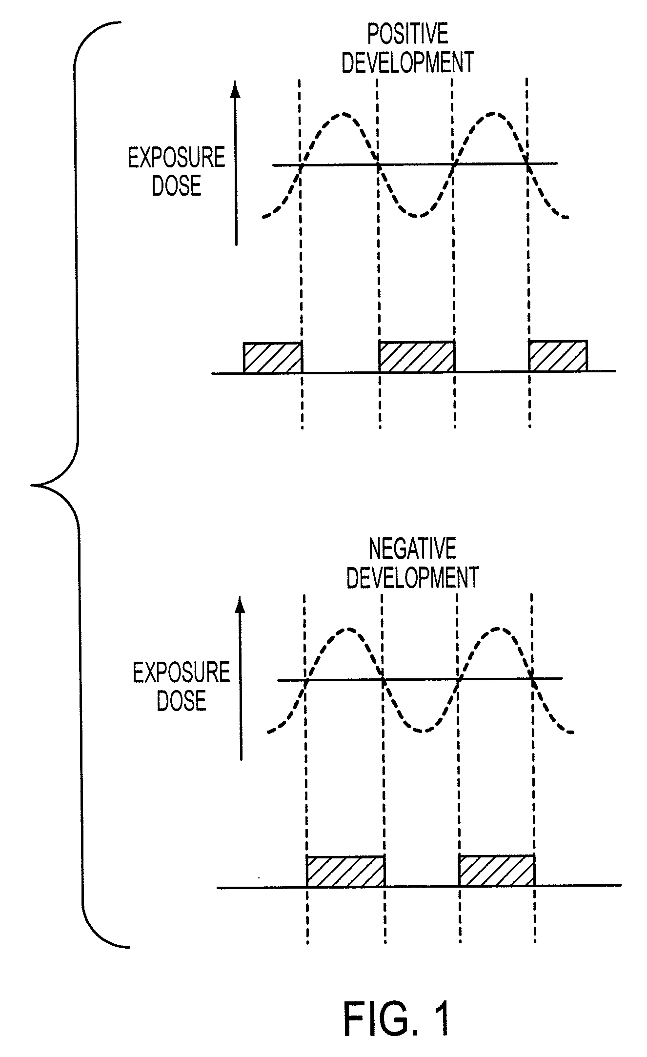
With the recent fine patterning, however, there arises a problem in the existing exposure system that light interference occurs in adjacent patterns and thus optical contrast is reduced.
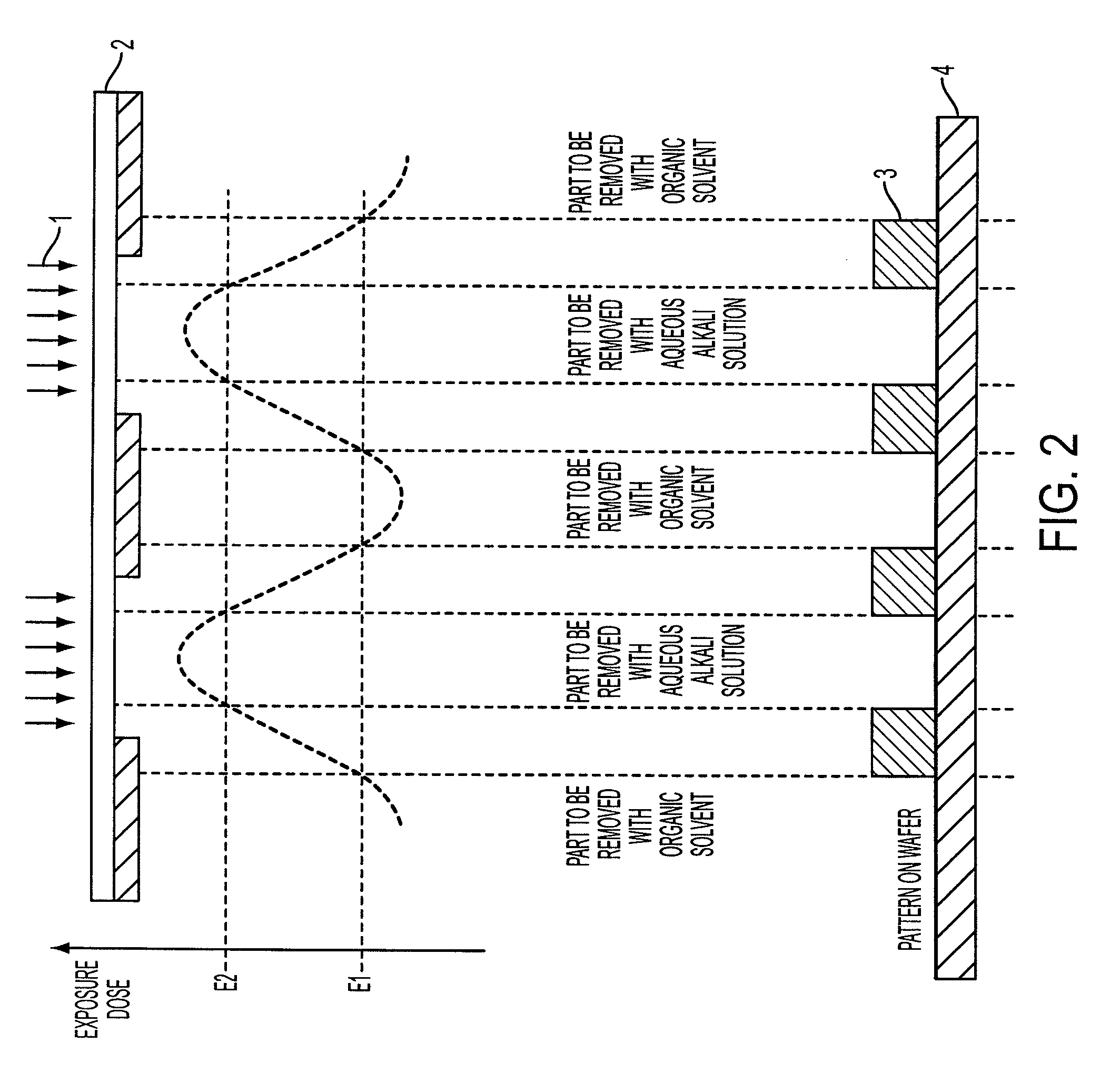
In the case where a pattern is formed merely by applying an existing resist composition to an existing resist process, there arises a problem that neither a sufficient exposure margin nor a sufficient focal depth can be obtained since the pattern should be formed in the vicinity of the limit of resolution of the resist in the double exposure system.
Namely, no sufficient resolution performance can be established by applying a pattern forming process which includes coating a substrate with a resist composition containing a resin showing an increase in polarity upon exposure, exposing, and developing by dissolving an exposed part of the resist film with an alkaline developing solution as reported in JP-A-2001-109154, etc., or a pattern forming process which includes coating a substrate with a resist composition containing a resin showing an increase in molecular weight upon exposure, exposing, and developing by dissolving a non-exposed part of the resist film with an alkaline developing solution as reported in JP-A-2003-76019, etc. to the double exposure system.
Therefore, it is impossible to express a sufficient change in polarity for causing a difference in dissolution characteristics due to the chemical amplification reaction accompanying exposure.
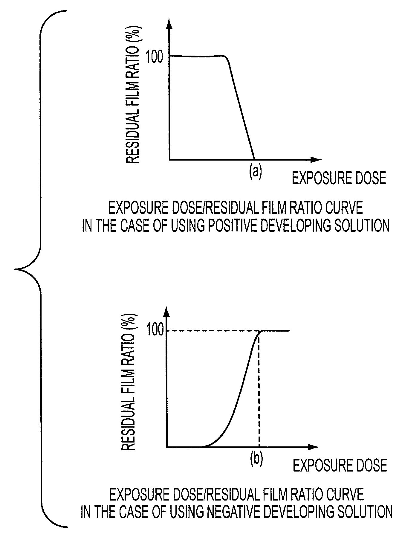
As a result, the development with the use of the negative developing solution proceeds at only a low development speed, which brings about a problem that the developing properties in using the negative developing solution are deteriorated.

Method used


Image

  • Pattern forming method, resist composition to be used in the pattern forming method, negative developing solution to be used in the pattern forming method and rinsing solution for negative development to be used in the pattern forming method
  • Pattern forming method, resist composition to be used in the pattern forming method, negative developing solution to be used in the pattern forming method and rinsing solution for negative development to be used in the pattern forming method
  • Pattern forming method, resist composition to be used in the pattern forming method, negative developing solution to be used in the pattern forming method and rinsing solution for negative development to be used in the pattern forming method

Examples


synthesis example 1

Synthesis of Resin (A1)

[0539]Into a three necked flask, 20 g of a solvent mixture including propylene glycol monomethyl ether acetate and propylene glycol monomethyl ether at a ratio (by mass) of 6 / 4 was introduced under a nitrogen gas stream and heated to 80° C. (solvent 1). γ-Butyrolactone methacrylate, hydroxyadamantane methacrylate and 2-methyl-2-adamantyl methacrylate were added at a molar ratio of 45 / 15 / 40 to s solvent mixture of propylene glycol monomethyl ether acetate and propylene glycol monomethyl ether at a ratio (by mass) of 6 / 4 to give a 22% by mass monomer solution (200 g). To this solution, 8% by mol of a polymerization initiator V-601 (manufactured by Wako Pure Chemical Industries, Ltd.) was added and dissolved. The resulting solution was dropped for 6 hours into the above solvent 1. After the completion of dropping, the reaction mixture was reacted for additional 2 hours at 80° C. Then, the liquid reaction mixture was cooled by standing and poured into hexane 1800 ...

example 1

[0548]An organic antireflective film ARC29A (manufactured by Nissan Chemical Industries, Ltd.) was coated on a silicon wafer and baked at 205° C. for 60 seconds to thereby form an antireflective film having a thickness of 78 nm. Then the resist composition (A1) was coated thereon and baked at 120° C. for 60 seconds to form a resist film having a thickness of 150 nm. The obtained wafer was subjected to pattern exposure with the use of an ArF excimer laser scanner (NA 0.75). After heating at 120° C. for 60 second, the wafer was subjected to (negative) development by the spray method with the use of butyl acetate (a negative developing solution) for 60 seconds under rotating at a rotational speed of 1000 rpm. Thus, a resist pattern of a 150 nm (1:1) line-and-space was obtained.

example 2

[0549]An organic antireflective film ARC29A (manufactured by Nissan Chemical Industries, Ltd.) was coated on a silicon wafer and baked at 205° C. for 60 seconds to thereby form an antireflective film having a thickness of 78 nm. Then the resist composition (A1) was coated thereon and baked at 120° C. for 60 seconds to form a resist film having a thickness of 150 nm. The obtained wafer was subjected to pattern exposure with the use of an ArF excimer laser scanner (NA 0.75). After heating at 120° C. for 60 second, the wafer was subjected to (negative) development by the spray method with the use of butyl acetate (a negative developing solution) for 60 seconds under rotating at a rotational speed of 1000 rpm. Next, the wafer was rinsed with 1-hexanol for 30 seconds while continuing the rotation. Then, the wafer was rotated at a rotational speed of 4000 rpm for 30 seconds to thereby remove the rinsing solution. Thus, a resist pattern of a 150 nm (1:1) line-and-space was obtained.


PUM

PropertyMeasurementUnit
Temperatureaaaaaaaaaa
Vapor pressureaaaaaaaaaa

Abstract

A pattern forming method includes (a) coating a substrate with a resist composition including a resin that includes a repeating unit represented by a following general formula (NGH-1), and, by the action of an acid, increases the polarity and decreases the solubility in a negative developing solution; (b) exposing; and (d) developing with a negative developing solution:wherein RNGH1 represents a hydrogen atom or an alkyl group; and RNGH2 to RNGH4 each independently represents a hydrogen atom or a hydroxyl group, provided that at least one of RNGH2 to RNGH4 represents a hydroxyl group.

Description

CROSS-REFERENCE TO RELATED APPLICATION[0001]This is a Continuation-In-Part application of U.S. application Ser. No. 12 / 102,504 filed in the United States on Apr. 14, 2008; the entire content of which is hereby incorporated by reference.BACKGROUND OF THE INVENTION[0002]1. Field of the Invention[0003]This invention relates to a pattern forming method which is usable in the course of producing semiconductors such as ICs, producing liquid crystals or circuit boards such as thermal heads and lithographing other photofabrications, a resist composition for negative development to be used in the pattern forming method, a resist composition for multiple development to be used in the pattern forming method, a negative developing solution to be used in the pattern forming method and a rinsing solution for negative development to be used in the pattern forming method. In particular, it relates to a pattern forming method appropriately usable in exposure with the use of an ArF exposure device an...

Claims


Application Information

Patent Timeline
IPC IPC(8): G03C1/053G03F7/20
CPCG03F7/325G03F7/0397Y10S430/106Y10S430/111
Inventor TSUBAKI, HIDEAKITARUTANI, SHINJIMIZUTANI, KAZUYOSHIWADA, KENJIHOSHINO, WATARU
Owner FUJIFILM CORP
Learn More