

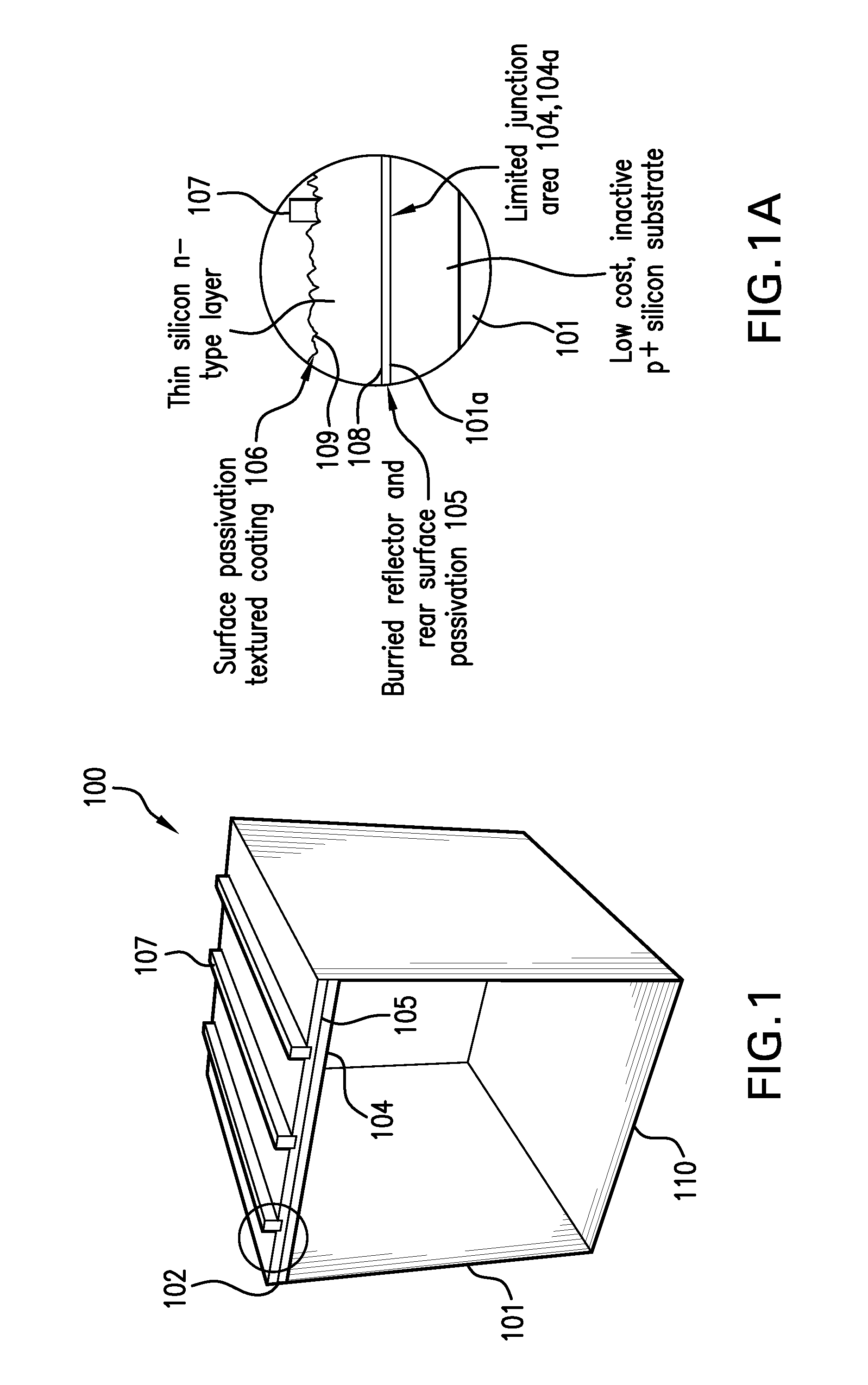
Photovoltaic Thin-Film Solar Cell and Method Of Making The Same
a technology of solar cells and thin films, applied in the manufacture of final products, basic electric elements, coatings, etc., can solve the problems of increased detrimental effects of defects, and achieve the effects of improving the performance of thin-film pv cells, increasing the resistance of substrates, and high efficiency
- Summary
- Abstract
- Description
- Claims
- Application Information
AI Technical Summary
Benefits of technology
Problems solved by technology
Method used
Image

Examples
example 1
[0134]This example demonstrates two thin film photovoltaic devices, one fabricated on a low-resistivity semiconductor-grade mono-crystalline silicon substrate (similar to the device seen in FIG. 5) and the other fabricated on a low resistivity and low cost Upgraded Metallurgical Grade (UMG) mono-crystalline silicon substrate (similar to device seen in FIG. 5). The device has an N-type epitaxial silicon layer with a front surface pyramidal texture on a P+ type mono-crystalline silicon substrate. The thin film epitaxial Si layers on both devices were of high quality, i.e. low defect density. FIG. 6 shows a defect density of a high quality epitaxial layer (2). The debris seen on the surface of the device in FIG. 5 is particles due to exposure to a non-cleanroom environment, not crystallographic defects.
[0135]The photovoltaic device on semiconductor grade silicon achieved an energy conversion efficiency of 14.80%, Open Circuit Voltage (Voc) of 0.6124 V, Short Circuit Current Density (Js...
example 2
[0139]This example describes the “fault tolerance” exhibited in thin film epitaxial photovoltaic devices that use a silicon substrate having a resistivity of 0.02 ohm-cm or greater. When defects such as stacking faults, dislocations point defects, or voids form in the thin film epitaxial layer, shunt paths occur that may degrade overall solar cell performance. By using a substrate in the mentioned resistivity range, these micro-shunts have been found to negligibly impact the overall device performance as evidenced in Voc measurements, a key measurement of solar cell performance. On the other hand, the performance of thin film photovoltaic devices using substrates below the stated resistivity range is negatively impacted by these faults and therefore these devices do not exhibit “fault tolerance.”
[0140]Following Si epitaxial chemical vapor deposition as in Example 1, the front (top) surface was preferentially etched to highlight crystallographic defects present in the N-type thin fil...
example 3
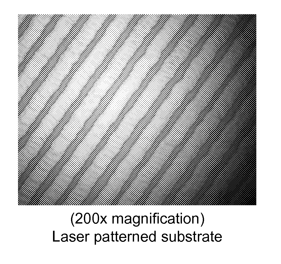
[0143]This example demonstrates the use of Si Epitalixial Laterial Overgrowth (ELO) as a means of creating a buried reflector at the junction area between the substrate and the N-type thin film epitaxial layer such as demonstrated in examples 1 and 2. This approach improves the light trapping optics of the cell and reduces recombination at the epitaxial silicon / substrate interface. In this example, laser patterning is employed as a potential cost-effective method to pattern the isolator-reflector layer before the silicon ELO deposition.
[0144]The buried reflector was created by coating a P-type substrate (resistivity: 0.1 ohm cm) with a thin SiNx layer of under 1000 angstroms, via Plasma Enhanced Chemical Vapor Deposition. A frequency-doubled Nd-YAG laser was then used to remove the SiNx layer and create line patterns. The lines were approximately 20 microns apart as shown on the photo (FIG. 9). Subsequently, an N-type ELO layer was created via silicon chemical vapor deposition, usin...
PUM
 Abstract
Description
Claims
Application Information