

Photovoltaic-Charged Secondary Battery System
a secondary battery and photovoltaic technology, applied in the direction of cell components, sustainable manufacturing/processing, semiconductor/solid-state device details, etc., can solve the problems of waste of surplus electric power, environmental destruction, and limitations to increase the capacity per unit volume and unit weight, so as to maximize energy efficiency
- Summary
- Abstract
- Description
- Claims
- Application Information
AI Technical Summary
Benefits of technology
Problems solved by technology
Method used
Image

Examples
example 1
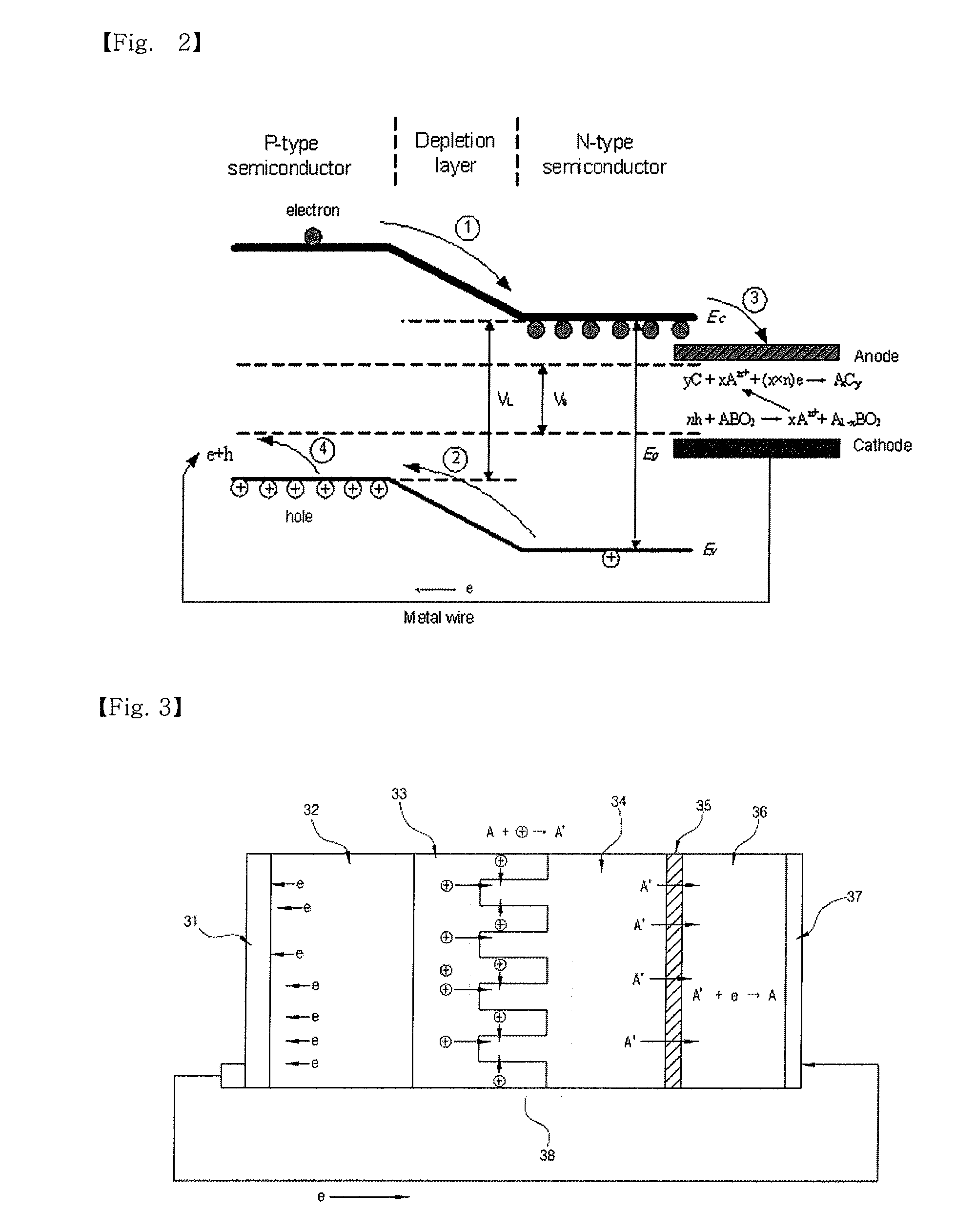
[0128]A photovoltaic-charged secondary battery system in accordance with the present Example generally had a multilayer structure, in which a lower electrode was formed on a lower flexible substrate, a light absorbing layer was formed thereon, a buffer layer was formed thereon, a window layer was formed thereon, and a secondary battery layer was formed thereon. In accordance with the present invention, a secondary battery anode layer was used as an upper electrode.
[0129]In order to form a transparent flexible lower electrode, indium tin oxide ITO was deposited on a high heat-resistant flexible substrate such as Arylite, colorless PI, or Upilex by sputtering, or fluorine-doped SnO2 was deposited in a thickness of 0.08 to 0.1 μm by the electron cyclotron resonance chemical vapor deposition (ECR-CVD) method, disclosed in Korean Patent No. 10-0613405. The lower electrode may be formed of any material forming a minimum contact resistance with or an ohmic contact with p-type Cu(In,Ga)(Se,...
example 2
[0136]A photovoltaic-charged secondary battery system in accordance with the present Example generally had a multilayer structure, in which a lower electrode was formed on a lower flexible substrate, a window layer was formed thereon, a buffer layer was formed thereon, a light absorbing layer was formed thereon, and a secondary battery layer was formed thereon. In accordance with the present invention, a secondary battery anode layer was used as an upper electrode.
[0137]In order to form a transparent flexible lower electrode, a pure metal or an alloy such as Al and AlNi was arranged in the form of a grid so that solar transmittance might be made maximally on a high heat-resistant flexible substrate such as Arylite, colorless PI, or Upilex by an electron beam evaporation method. Al layer of above 2 μm was used to reduce resistance and Ni of about 50 to 100 nm was disposed therebelow to reduce contact resistance.
[0138]The n-type semiconductor window layer was fabricated by forming ZnO...
example 3
[0142]In order to improve the photoelectric conversion efficiency, the below-described method was employed to manufacture an n-type semiconductor having a large surface area. As the cathode layer, Li1-xMn2O4 from which lithium was removed was used and, as the anode layer, LeCoO2 was used. The manufacturing method was the same as Example 1. The charge / discharge curves of the secondary battery layer are shown in FIG. 14, in which a flat potential of about 0.3 V is shown. The cathode and anode active materials may be selected from the aforementioned group other than those described in the present Example.
[0143]A polymer templating technique was employed to form a porous metal oxide semiconductor layer, in which the specific surface area was significantly increased, as described below.
[0144]First, PMMA beads having a diameter of 800 nm were dispersed. Here, the diameter of the beads may be varied. The PMMA beads (Soken Chemical & Engineering Co., Ltd.) having a concentration in a range ...
PUM
| Property | Measurement | Unit |
|---|---|---|
| charging capacity | aaaaa | aaaaa |
| charging capacity | aaaaa | aaaaa |
| driving voltage | aaaaa | aaaaa |
Abstract
Description
Claims
Application Information