[0013]In accordance with one aspect of the present invention, the foregoing and other objects are achieved by fabrication of self-assembled, crystalline nanodots and nanorods of a certain composition within a crystalline matrix of another phase. As used herein, the
phrase “self-assembled” is defined herein to mean a self-ordering process wherein the ordering occurs naturally during growth of the
composite material or film. In particular, the invention enables fabrication of high performance and novel, electrical, magnetic, electromagnetic and electrooptical devices via epitaxial deposition on
single crystal and / or
single crystal-like, biaxially textured substrates by incorporation of self-assembled nanodots and nanorods of a second phase material within a device layer.
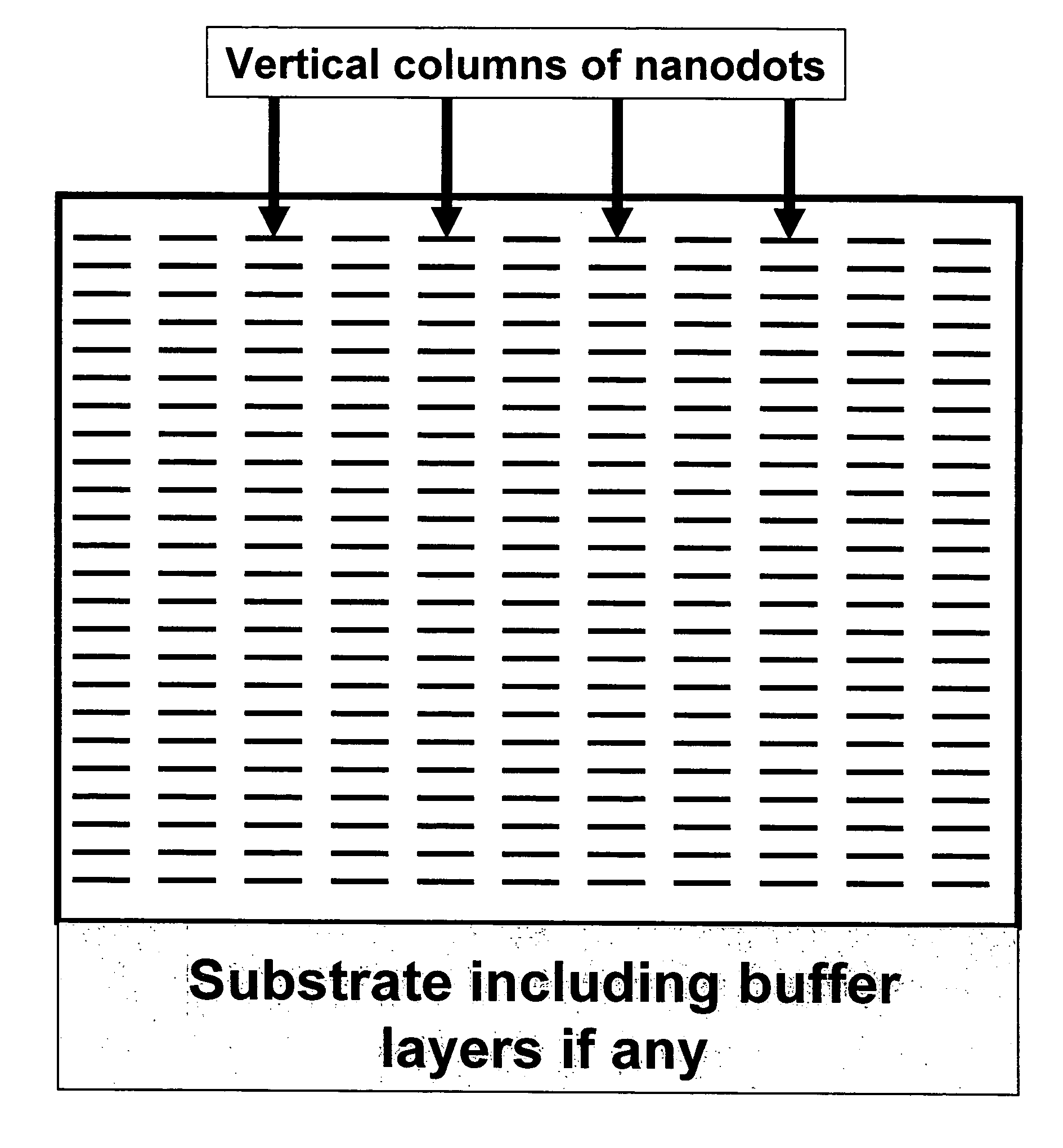
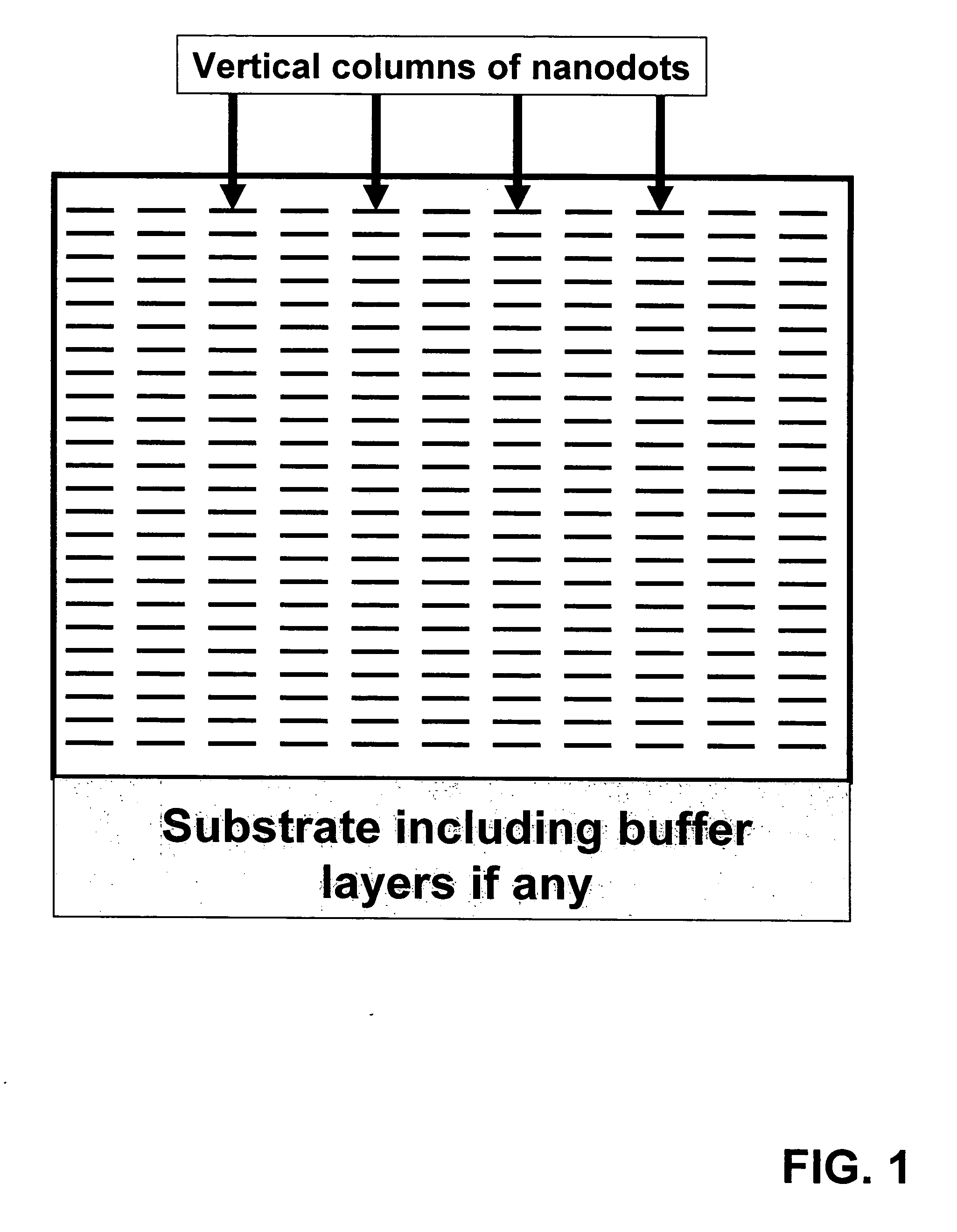
[0018]In accordance with another aspect of the present invention, the foregoing and other objects are achieved by fabrication of a high-temperature superconducting tape consisting of atleast one superconducting layer having columns of aligned nanodots of a non-
superconducting material, with the
diameter of nanodots being in the range of 2-100 nanometers. The invention allows results in over 80% of the non-superconducting nanodots aligned within 60 degrees from the c-axis of superconductor. The invention also allows for further having defects perpendicular to the c-axis of the superconductor selected from a group comprising of aligned second phase particles and stacking faults. The invention provides for epitaxial deposition of the superconductor on a biaxially textured substrate selected from a group comprising of
single crystal substrates, IBAD textured substrates, ISD textured substrates and thermomechanically textured substrates. Formation of non-superconducting, self-assembled nanodots and nanodots occurs due to strain minimization because of lattice mismatch between the non-superconducting nanodots and nanorods and the superconductor film.
[0019]In accordance with another aspect of the present invention, the foregoing and other objects are achieved by fabrication of an electrical, electronic, magnetic or electromagnetic composite device layer consisting of atleast one layer of a certain crystalline composition with aligned nanodots of another crystalline composition, with the
diameter of nanodots being in the range of 2-100 nanometers. The invention provides for over 80% of the nanodots aligned within 60 degrees from the normal to the device layer. The invention further allows for the device layer to have more than one cation constituent. The invention also allows for the embedded, self-assembled nanodots and / or nanorods to have more than one cation constituent. The invention provides for epitaxial deposition of the composite device layer on a biaxially textured substrate selected from a group comprising of single
crystal substrates, IBAD textured substrates, ISD textured substrates and thermomechanically textured substrates. Formation of the second-phase phase array ordered array of self-assembled nanodots and nanodots occurs due to strain minimization because of lattice mismatch between the second-phase, nanodots and nanorods and the matrix film. The invention includes composite device
layers for photovoltaic, ferroelectric, and magnetic applications. The invention also provides for fabrication of composite device
layers to be used as an array of light emitting diodes for
solid state lighting applications. The invention also allows for device layer is used for storage applications such as
computer hard disc drives. The invention also allows for the device layer to exhibit
photoluminescence. The invention also allows for the device layer to exhibit
magnetoresistance. The invention also allows for the device layer to exhibit
superconductivity. The invention further allows for all the nanodots to merge forming an array of nanorods. The invention also allows for all the presence of an array of both nanodots and nanorods.
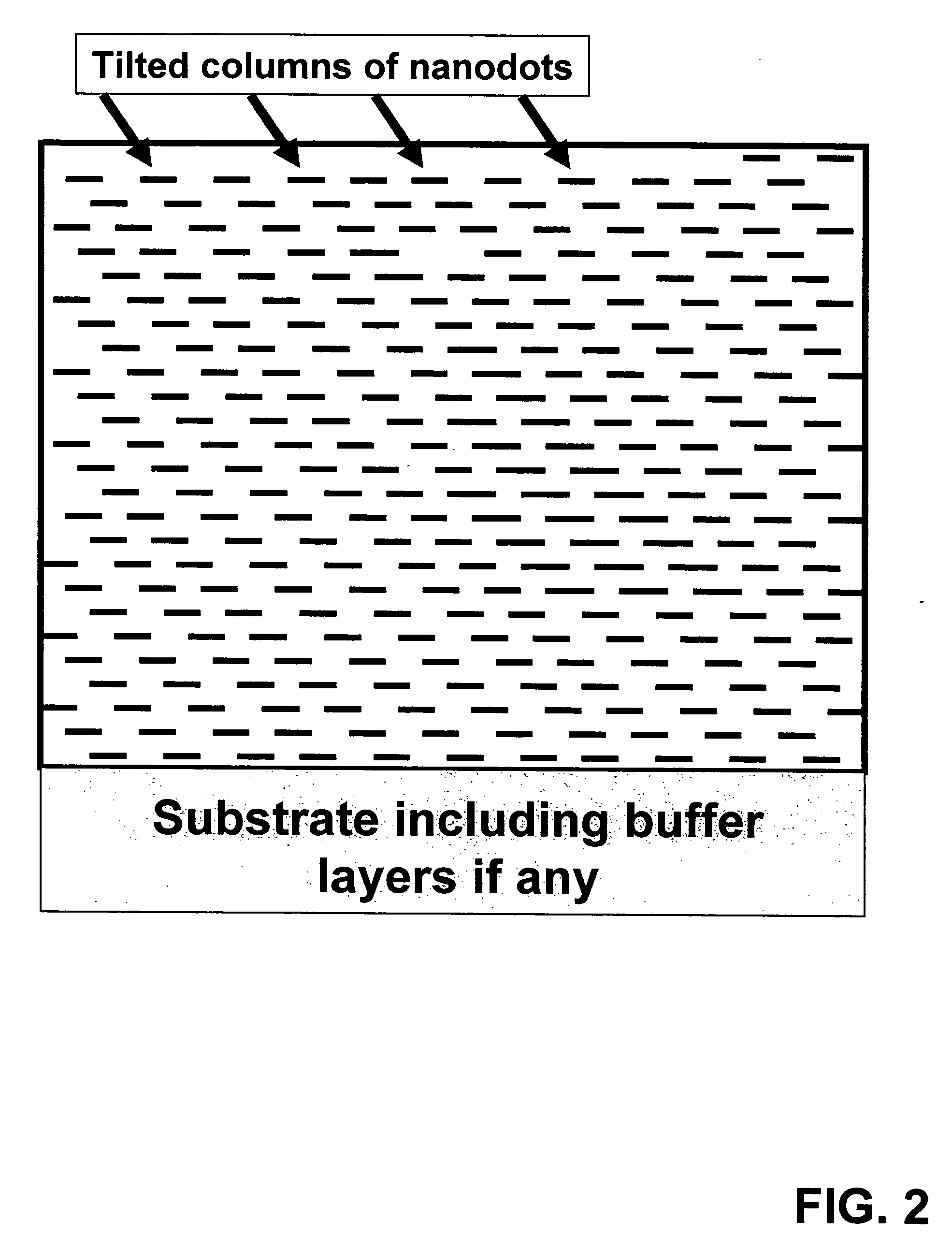
[0020]In accordance with another aspect of the present invention, the foregoing and other objects are achieved by fabrication of an electrical, electronic, magnetic or electromagnetic composite device layer consisting of atleast one layer of a certain crystalline composition with aligned columns of another crystalline composition, with the
diameter of columns being in the range of 2-100 nanometers. The invention provides for over 80% of the nanodots aligned within 60 degrees from the normal to the device layer. The invention further allows for the device layer to have more than one cation constituent. The invention also allows for the embedded, self-assembled nanodots and / or nanorods to have more than one cation constituent. The invention provides for epitaxial deposition of the composite device layer on a biaxially textured substrate selected from a group comprising of single
crystal substrates, IBAD textured substrates, ISD textured substrates and thermomechanically textured substrates. Formation of the second-phase array ordered array of self-assembled nanodots and nanodots occurs due to strain minimization because of lattice mismatch between the second-phase, nanodots and nanorods and the matrix film. The invention includes composite device layers for photovoltaic, ferroelectric, and magnetic applications. The invention also provides for fabrication of composite device layers to be used as an array of light emitting diodes for
solid state lighting applications. The invention also allows for device layer is used for storage applications such as
computer hard disc drives. The invention also allows for the device layer to exhibit
photoluminescence. The invention also allows for the device layer to exhibit
magnetoresistance. The invention also allows for the device layer to exhibit
superconductivity. The invention further allows for all the nanodots to merge forming an array of nanorods. The invention also allows for all the presence of an array of both nanodots and nanorods.
[0021]In accordance with another aspect of the present invention, the foregoing and other objects are achieved by fabrication of a composite
dielectric layer consisting of atleast one layer of a certain composition with aligned nanodots and / or nanorods of another composition, with the diameter of nanodots and / or nanorods being in the range of 2-100 nanometers. The invention provides for over 80% of the nanodots aligned within 60 degrees from the normal to the device layer. The invention further allows for the device layer to have more than one cation constituent. The invention also allows for the embedded, self-assembled nanodots and / or nanorods to have more than one cation constituent. The invention provides for epitaxial deposition of the composite device layer on a biaxially textured substrate selected from a group comprising of single
crystal substrates, IBAD textured substrates, ISD textured substrates and thermomechanically textured substrates. Formation of the second-phase array ordered array of self-assembled nanodots and nanodots occurs due to strain minimization because of lattice mismatch between the second-phase, nanodots and nanorods and the matrix film.

