Method for manufacturing semiconductor substrate

Inactive Publication Date: 2009-04-09
SEMICON ENERGY LAB CO LTD
View PDF25 Cites 19 Cited by
  • Summary
  • Abstract
  • Description
  • Claims
  • Application Information

AI Technical Summary

Benefits of technology

[0018]In the method for manufacturing a semiconductor substrate of the present invention, a second single crystal semiconductor substrate obtained after the separation is irradiated and scanned with CW laser light having a suitable wavelength, so that the planarity of a surface of the second single crystal semiconductor substrate can be recovered. In addition, by recovering the planarity of the surface of the second single crystal semiconductor substrate, the second single crystal semiconductor substrate can be used again for manufacturing a semiconductor substrate. Further, by using the reprocessed second single crystal semicon

Problems solved by technology

However, planarity of a surface of a single crystal semiconductor substrate from which thin films of single crystal silicon layers are separated by a hydrogen ion i

Method used


Image

  • Method for manufacturing semiconductor substrate
  • Method for manufacturing semiconductor substrate
  • Method for manufacturing semiconductor substrate

Examples


embodiment modes

[0036]An example of a manufacturing method of a semiconductor substrate in Embodiment Modes of the present invention will now be described with reference to drawings. However, the present invention can be embodied in many different modes and it is easily understood by those skilled in the art that the mode and detail thereof can be variously changed without departing from the scope and spirit of the present invention. Accordingly, the present invention should not be interpreted as being limited to the description of the embodiment modes.

embodiment mode 1

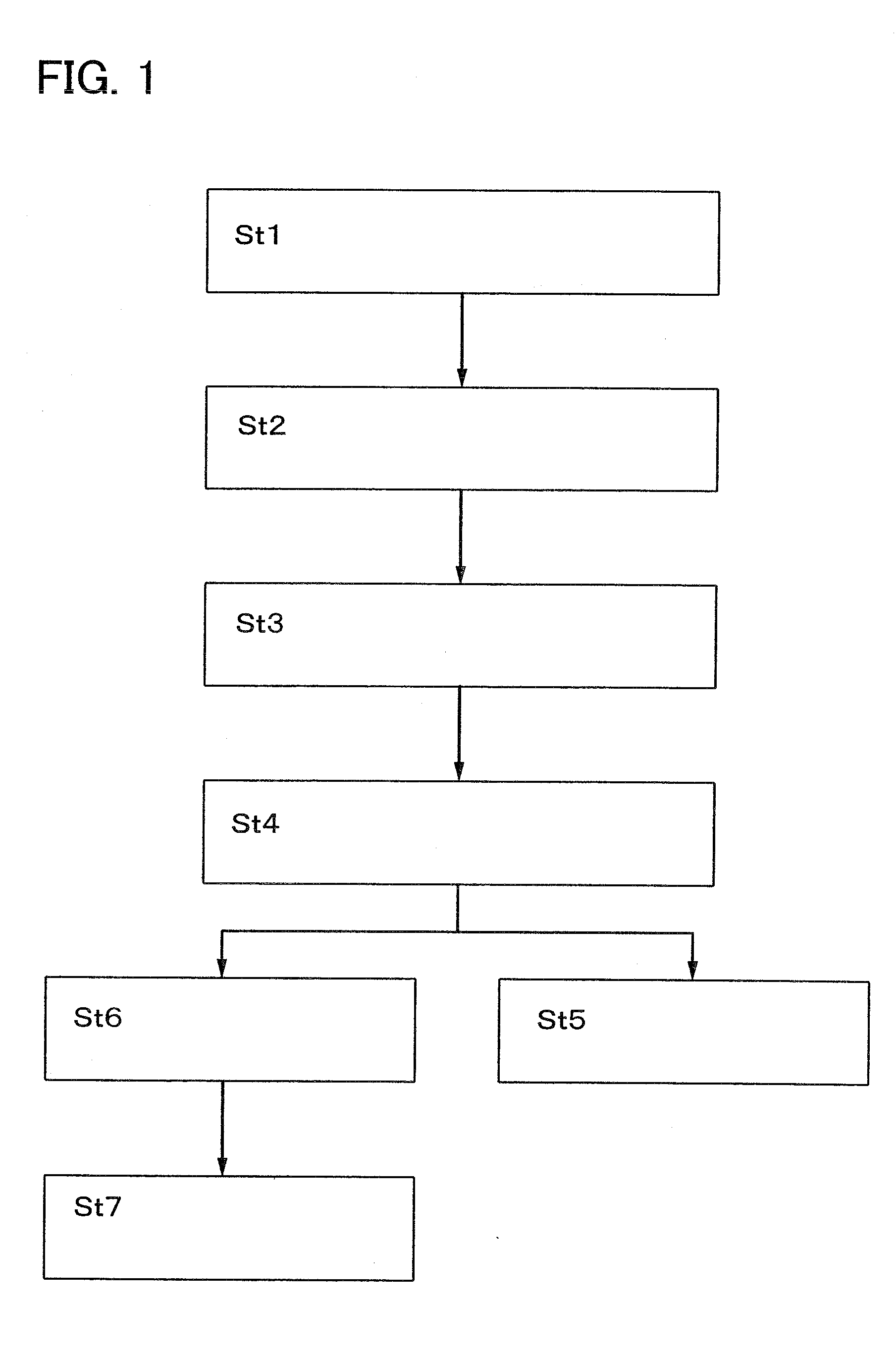
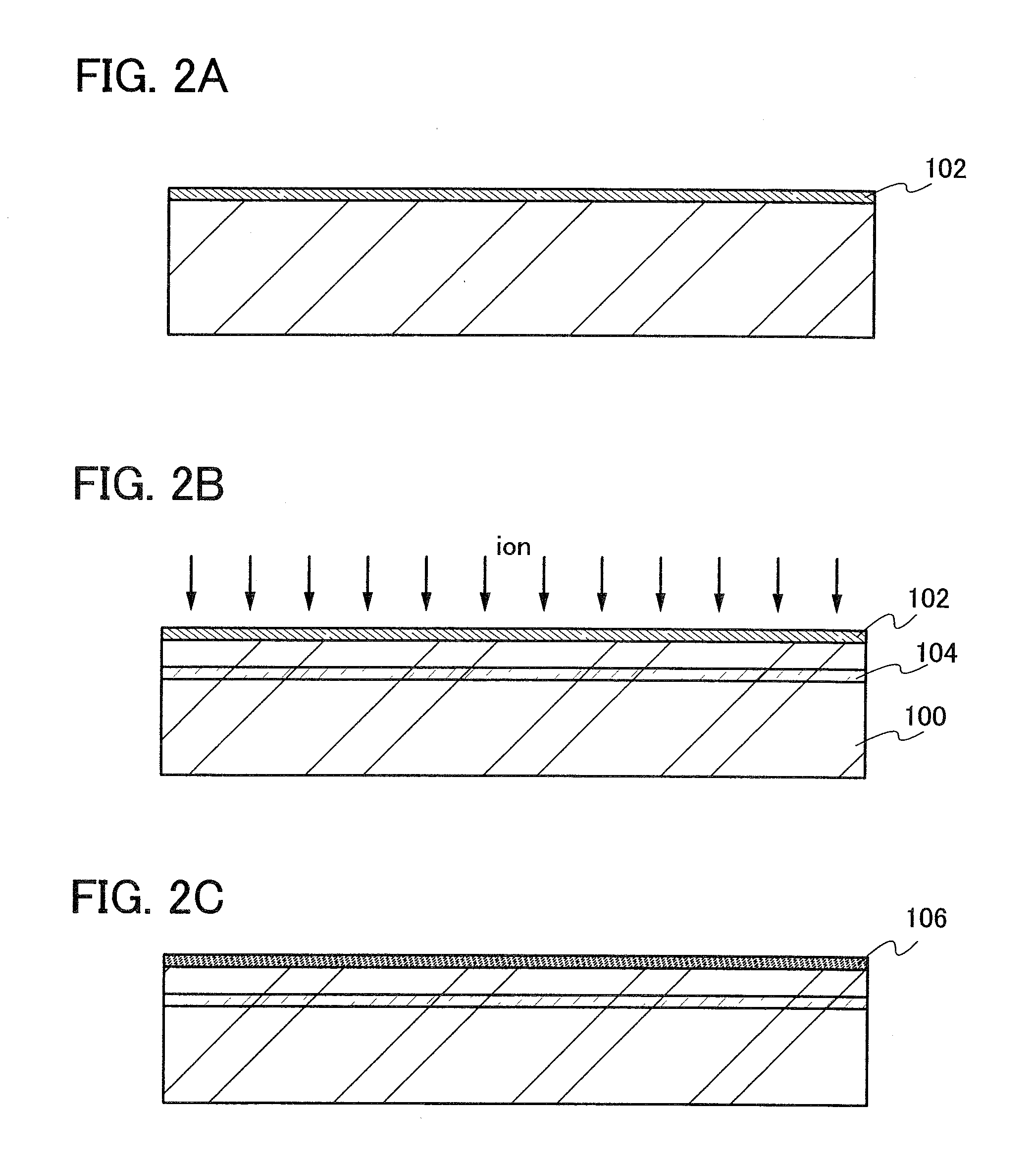
[0037]The present invention relates to a planarization process of a single crystal semiconductor substrate after a thin film of single crystal semiconductor layer is separated from the single crystal semiconductor substrate. FIG. 1 is a flow chart illustrating a manufacturing process of a semiconductor substrate according to the present invention, as an example.

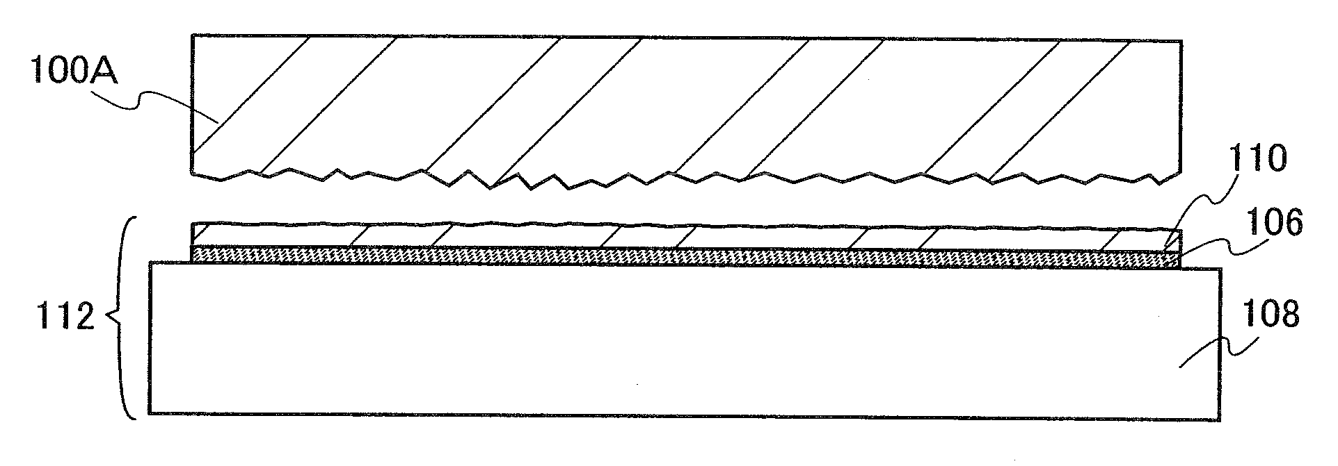
[0038]First, a protective film is formed over a single crystal semiconductor substrate and the single crystal semiconductor substrate is irradiated with an ion beam through the protective film to form an embrittlement layer (ion-implantation layer) (St 1). Then, a bonding layer is formed over the single crystal semiconductor substrate or a base substrate (St 2), and the single crystal semiconductor substrate and the base substrate are bonded to each other (St 3). Then, the single crystal semiconductor substrate is separated from the base substrate by heat treatment, using the embrittlement layer as a cleavage plane (St 4) and...

embodiment mode 2

[0083]In the method for manufacturing a semiconductor substrate described with reference to FIG. 1, FIGS. 2A to 2C, FIGS. 3A and 3B, and FIGS. 4A and 4B, if a base substrate having an upper temperature limit of 700° C. or lower such as glass is used, a bonding strength with a single crystal semiconductor substrate can be strengthened. Further, a wide variety of kinds of glass substrates such as a non-alkaline glass substrate can be applied for the base substrate. Accordingly, by using a glass substrate as the base substrate, a semiconductor substrate with a large size whose one side is more than one meter can be manufactured. When a plurality of semiconductor elements are provided for such a large-sized semiconductor substrate, a liquid crystal display and an electroluminescent display can be manufactured. In addition to such display devices, various kinds of semiconductor devices such as a solar cell, a photo IC, and a semiconductor memory device can be manufactured using a semicon...


PUM


Abstract

When a single crystal semiconductor layer is bonded to a base substrate, a silicon oxide film is preferably used for one or both of the base substrate and a single crystal semiconductor substrate. According to this structure, an SOI layer having a strong bonding strength in a bonding portion can be obtained even when a substrate having an upper temperature limit of 700° C. or lower such as a glass substrate is used. In addition, a single crystal semiconductor substrate from which the single crystal semiconductor layer has been separated is reprocessed in such a manner that the single crystal semiconductor substrate is irradiated with laser light from the separation surface side of the single crystal semiconductor substrate, to melt the surface of the single crystal semiconductor substrate during the melting time per area of 0.5 microseconds to 1 millisecond. Then, the reprocessed single crystal semiconductor substrate is reused.

Description

BACKGROUND OF THE INVENTION[0001]1. Field of the Invention[0002]The present invention relates to a method for manufacturing a semiconductor substrate having a semiconductor layer on its insulating surface.[0003]2. Description of the Related Art[0004]In recent years, a technique for forming a thin film transistor (TFT) using a semiconductor thin film (the thickness of several nm to several hundreds of nm) formed over a substrate having an insulating surface such as glass has been attracted. Thin film transistors are applied to a wide range of electronic devices like integrated circuits and electro-optical devices, and prompt development of thin film transistors that are to be used as switching elements in image display devices, in particular, is being pushed.[0005]Instead of silicon wafers that are manufactured by thinly slicing an ingot of a single crystal semiconductor, semiconductor substrates called silicon-on-insulator (SOI) substrates have been developed, which have a thin sing...

Claims


Application Information

Patent Timeline
IPC IPC(8): H01L21/30
CPCH01L21/02032H01L21/76254H01L21/268H01L21/20
Inventor MORIWAKA, TOMOAKI
Owner SEMICON ENERGY LAB CO LTD
Why Eureka
Try Eureka