Methods to obtain low k dielectric barrier with superior etch resistivity

a dielectric barrier and resistivity technology, applied in the field of integrated circuit fabrication, can solve the problems of short circuit formation and device failure, loss of etch selectivity and barrier property, etc., and achieve the effects of low ultra-violent absorption, high etching resistance, and low dielectric constan

Inactive Publication Date: 2009-04-09
APPLIED MATERIALS INC
View PDF10 Cites 39 Cited by
  • Summary
  • Abstract
  • Description
  • Claims
  • Application Information

AI Technical Summary

Benefits of technology

[0068]The dielectric barrier film of the present invention has several advantages over conventional barrier film, for example, high etching resistance, low dielectric constant, low ultra violent absorption, high diffusion barrier, and hydrophobic. The advantages of the film not only make it a better barrier when used as a traditional barrier film, but also enable novel applications.

Problems solved by technology

However, low k dielectric materials are often susceptible to interlayer diffusion of conductive materials, such as copper, which can result in the formation of short circuits and device failure.
However, conventional approaches for introducing porosity to barrier layers usually result in loss in etch selectivity and barrier property.

Method used


Image

  • Methods to obtain low k dielectric barrier with superior etch resistivity
  • Methods to obtain low k dielectric barrier with superior etch resistivity
  • Methods to obtain low k dielectric barrier with superior etch resistivity

Examples


example 1

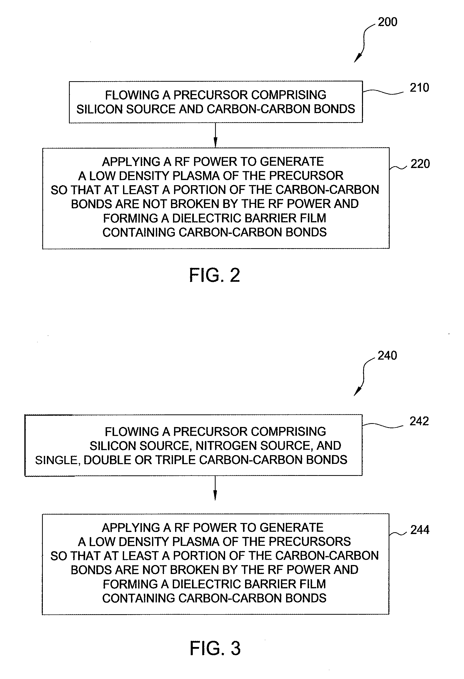
[0054]A PECVD deposition process for depositing a porous dielectric layer comprising silicon carbide using a precursor comprising the combination of trimethylsilane (TMS, (CH3)3SiH) and ethylene (C2H4). A carrier gas, such as helium, argon, nitrogen, or combinations thereof, is introduced with the precursor to the processing chamber.

[0055]The ratio of TMS and ethylene is set such that the atomic percentage of carbon of the mixture is greater than 15%. In one embodiment, the ratio of ethylene and TMS is between about 0.5:1 to about 8:1. In another embodiment, the ratio of ethylene and TMS is between about 1:1 to about 4:1. The processing parameters are as follows:

[0056]Flow rate (including precursor and carrier gas): between about 5 sccm to about 10,000 sccm, wherein the flow rate of carrier gas may be between about 5 sccm to about 10,000 sccm.

[0057]Spacing: from about 200 mils to about 2000 mils;

[0058]Temperature: between about 100° C. to about 550° C., or between about 200° C. to a...

example 2

[0061]A PECVD deposition process for depositing a porous dielectric layer comprising silicon carbide using a precursor comprising the combination of trimethylsilane (TMS, (CH3)3SiH), ethylene (C2H4) and ammonia (NH3). In one embodiment, the ratio of ethylene and TMS is between about 3:1 to about 5:1. The ratio of ammonia and TMS may be between about 1:10 to about 10:1. In another embodiment, the ratio of ammonia and TMS may be between about 1:4 to about 3:1. The processing parameters are as follows:

[0062]Flow rate (including precursor and carrier gas): between about 5 sccm to about 10,000 sccm, wherein the flow rate of carrier gas may be between about 5 sccm to about 10,000 sccm.

[0063]Spacing: from about 200 mils to about 2000 mils;

[0064]Temperature: between about 100° C. to about 550° C., or between about 200° C. to about 350° C.;

[0065]Chamber pressure: between about 10 mTorr to one atmosphere;

[0066]RF power: from about 15 W to about 3,000 W. In one embodiment, the RF power may be ...

example 3

[0067]A PECVD deposition process for depositing a porous dielectric barrier using a precursor comprising the combination of trimethylsilane (TMS, (CH3)3SiH) and ethylene (C2H4). The process conditions, including the ratio of TMS and ethylene, are set such that the atomic percentage of carbon is greater than 15%. In one embodiment, the ratio of ethylene and TMS is about 1:1 to about 8:1, the flow rate of the TMS / ethylene precursor and carrier gas is between about 5 sccm to about 10,000 sccm, and the temperature is about 350° C. For these conditions, the chamber pressure is between about 10 mTorr to about one atmosphere, the radio frequency (RF) power for plasma generation is between about 15 W to about 3,000 W, and the spacing between a substrate and a shower head, configured for providing precursors to the substrate being processed, is from about 200 mils to about 2000 mils.

Advantages of the Barrier

[0068]The dielectric barrier film of the present invention has several advantages ove...


PUM

PropertyMeasurementUnit
feature sizesaaaaaaaaaa
dielectric constantsaaaaaaaaaa

Abstract

The present invention generally provides a method for forming a dielectric barrier with lowered dielectric constant, improved etching resistivity and good barrier property. One embodiment provides a method for processing a semiconductor substrate comprising flowing a precursor to a processing chamber, wherein the precursor comprises silicon-carbon bonds and carbon-carbon bonds, and generating a low density plasma of the precursor in the processing chamber to form a dielectric barrier film having carbon-carbon bonds on the semiconductor substrate, wherein the at least a portion of carbon-carbon bonds in the precursor is preserved in the low density plasma and incorporated in the dielectric barrier film.

Description

BACKGROUND OF THE INVENTION[0001]1. Field of the Invention[0002]Embodiments of the present invention generally relate to the fabrication of integrated circuits. More particularly, embodiments of the present invention relate to methods for forming a dielectric barrier film used in manufacturing semiconductor devices.[0003]2. Description of the Related Art[0004]Integrated circuit geometries have dramatically decreased in size since such devices were first introduced several decades ago. Since then, integrated circuits have generally followed the two year / half-size rule (often called Moore's Law), which means that the number of devices on a chip doubles every two years. Today's fabrication facilities are routinely producing devices having 0.1 μm feature sizes, and tomorrow's facilities soon will be producing devices having even smaller feature sizes.[0005]The continued reduction in device geometries has generated a demand for films having low dielectric constant (k) values because the ...

Claims


Application Information

Patent Timeline
Patent Type & Authority Applications(United States)
IPC IPC(8): H01L21/31
CPCC23C16/22C23C16/505H01L21/3185H01L21/3148H01L21/3121H01L21/0217H01L21/02167H01L21/02274H01L21/02205H01L21/02203H01L21/02211H01L21/31H01L21/02112
Inventor XU, HUIWENLIU, YIJUNXIA, LI-QUNWITTY, DEREK R.M'SAAD, HICHEM
Owner APPLIED MATERIALS INC
Why Eureka
Try Eureka