Method for fabricating semiconductor layer and light-emitting diode

a technology of light-emitting diodes and semiconductor layers, which is applied in the direction of polycrystalline material growth, chemistry apparatus and processes, crystal growth processes, etc., can solve the problems of unable to produce a gan layer exhibiting good quality, unable to stably form the semiconductor layer, and unable to achieve good quality. gan layer, the effect of reducing density and excellent lattice matching

Inactive Publication Date: 2009-05-21
SHOWA DENKO KK
View PDF3 Cites 5 Cited by
  • Summary
  • Abstract
  • Description
  • Claims
  • Application Information

AI Technical Summary

Benefits of technology

[0019]Further, since this invention contemplates using a boron phosphide layer as a first semiconductor layer and forming a Group III nitride semiconductor layer bonded thereto as a second semiconductor layer, it is capable of overcoming the inferior “wetting” property revealed between the boron phosphide layer and the Group III nitride semiconductor layer and consequently realizing formation of a Group III nitride semiconductor layer containing crystal defects only in a small density and excelling in quality.
[0020]Particularly since this invention further contemplates using as a first semiconductor layer a layer of excellent quality formed on a silicon single crystal substrate and made of a monomer boron phosphide inducing domain matching with the silicon single crystal and forming a Group III nitride semiconductor layer bonded thereto as a second semiconductor layer, it is capable of causing both these layers of excellent lattice matching property to be mutually bonded in a state exhibiting a high “wetting” property and consequently realizing formation of a Group III nitride semiconductor layer excelling in crystallinity.
[0021]Since this invention contemplates using a semiconductor layer having a surface formed of a crystal face of {001} as a first semiconductor layer and forming a Group III nitride semiconductor layer by irradiating the surface of the {001} crystal face with electrons, it is capable of efficiently forming a cubic Group III nitride semiconductor layer in a stable manner.
[0022]Since this invention, in forming a second semiconductor layer on the surface of a first semiconductor layer, further contemplates forming the second semiconductor layer while causing the electrons directed toward the surface of the first semiconductor layer to be decreased in density with time from the start of the growth of the second semiconductor layer onward, it is capable of enhancing the “wetting” property revealed between the first semiconductor layer and the second semiconductor layer, keeping the second semiconductor layer from sustaining uncalled-for damage owing to the radiation of electrons over a long time as well, and consequently forming a Group III nitride semiconductor layer of excellent quality.
[0023]Particularly, since this invention, in forming a second semiconductor layer on the surface of the first semiconductor layer and after starting the growth of the second semiconductor layer aimed at a thickness of t, contemplates stopping the radiation of electrons directed toward the surface of the first semiconductor layer before the thickness of the second semiconductor layer reaches 0.5 t, it is capable of keeping the second semiconductor layer from sustaining uncalled-for damage owing to the radiation of electrons over a long time and consequently forming a Group III nitride semiconductor layer of excellent quality.
[0024]Further, since this invention, in forming on the surface of a first semiconductor layer possessing a first ionicity a second semiconductor layer possessing a second ionicity larger than the first ionicity, contemplates forming the second semiconductor layer while irradiating the surface of the first semiconductor layer existing on the side for forming the second semiconductor layer with electrons in a vacuum and fulfilling the production of a light-emitting diode by using the resultant semiconductor layers, it is capable of enabling the component layers of the light-emitting diode to decrease twin crystals and stacking faults to a small density, excel in crystallinity and exhibit enhancement in luminance of emission, reverse voltage and breakdown voltage.

Problems solved by technology

The problem exists that the semiconductor layer cannot be stably formed.
No success has been achieved in producing a GaN layer exhibiting good quality and containing crystal defects only in a small density.

Method used


Image

  • Method for fabricating semiconductor layer and light-emitting diode
  • Method for fabricating semiconductor layer and light-emitting diode

Examples


example 1

[0055]This invention will be specifically described with reference to the case of forming a cubic GaN layer while simultaneously radiating an electron beam on a silicon carbide layer formed on a (001) crystal face constituting the surface of a (001)-silicon single crystal substrate.

[0056]A phosphorus (P)-doped n-type Si single crystal substrate was conveyed at room temperature into the growth chamber of a molecular beam epitaxial (MBE) growth device. The substrate was subsequently heated in a high vacuum of about 1×10⁻⁷ Pa to 1050° C. The fact that the heat treatment of the substrate at the high temperature in the high vacuum induced a (2×1) reconstruction structure of a (001) crystal face constituting the surface of the substrate was confirmed by an ordinary reflection high-energy electron diffraction (RHEED).

[0057]Thereafter, the temperature of the silicon single crystal substrate was lowered to 490° C. while the high vacuum was retained constant. After the temperature of the subs...

example 2

[0063]This invention will be specifically described with reference to the case of forming a hexagonal AlGaN layer while simultaneously radiating an electron bean on a silicon carbide layer formed on a (111) crystal face constituting the surface of a (111)-silicon single crystal substrate.

[0064]A boron (B)-doped p-type Si single crystal substrate was conveyed at room temperature into the growth chamber of a molecular beam epitaxial (MBE) growth apparatus. Then, the substrate was heated in a high vacuum of about 1×10⁻⁷ Pa to 850° C. The fact that the heat treatment of the substrate at the high temperature in the high vacuum induced a (7×7) reconstruction structure of a (111) crystal face constituting the surface of the substrate was confirmed by an ordinary reflection high-energy electron diffraction (RHEED).

[0065]Thereafter, the temperature of the silicon single crystal substrate was lowered to 490° C. while the high vacuum was retained constant. After the temperature of the substrat...

example 3

[0070]The effect of the present invention will be specifically described with reference to the case of manufacturing a Group III nitride semiconductor light-emitting diode utilizing a GaN layer formed while continuing radiation of electrons as in Example 1.

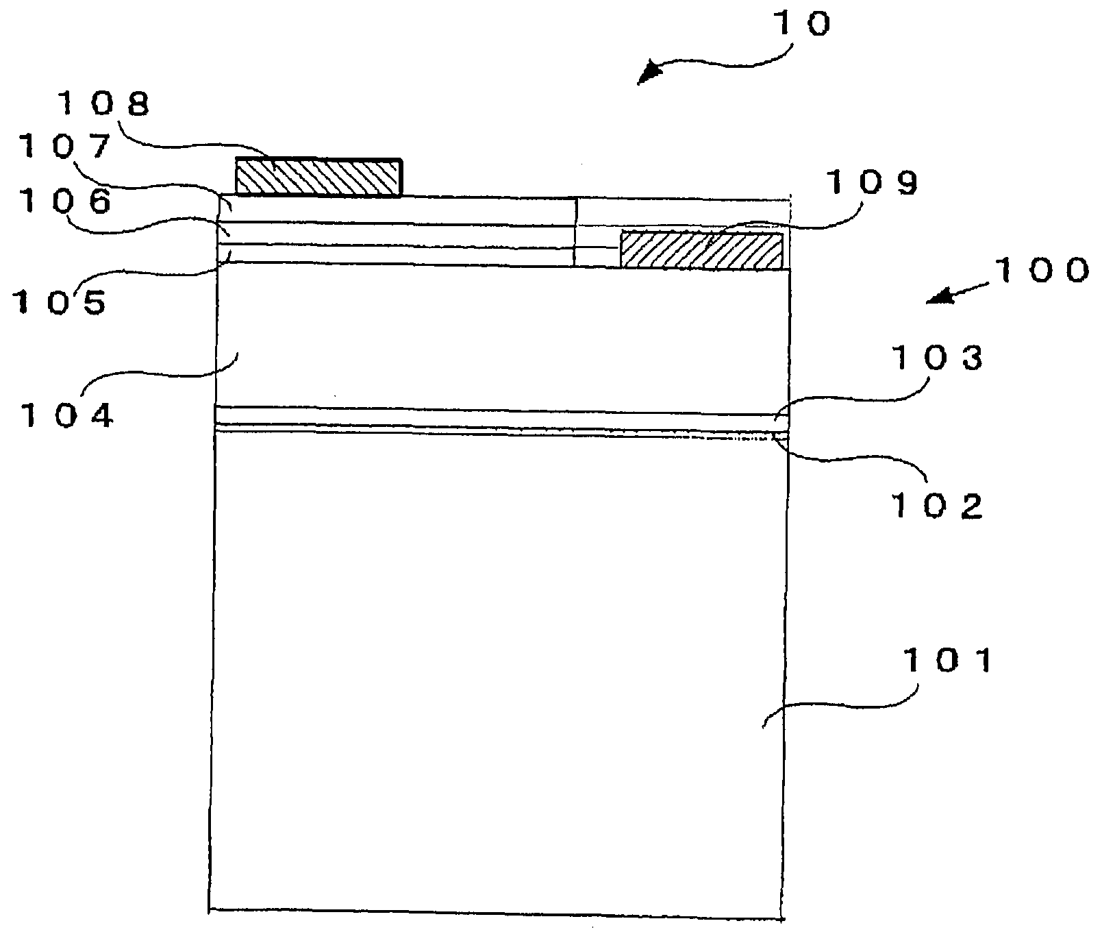
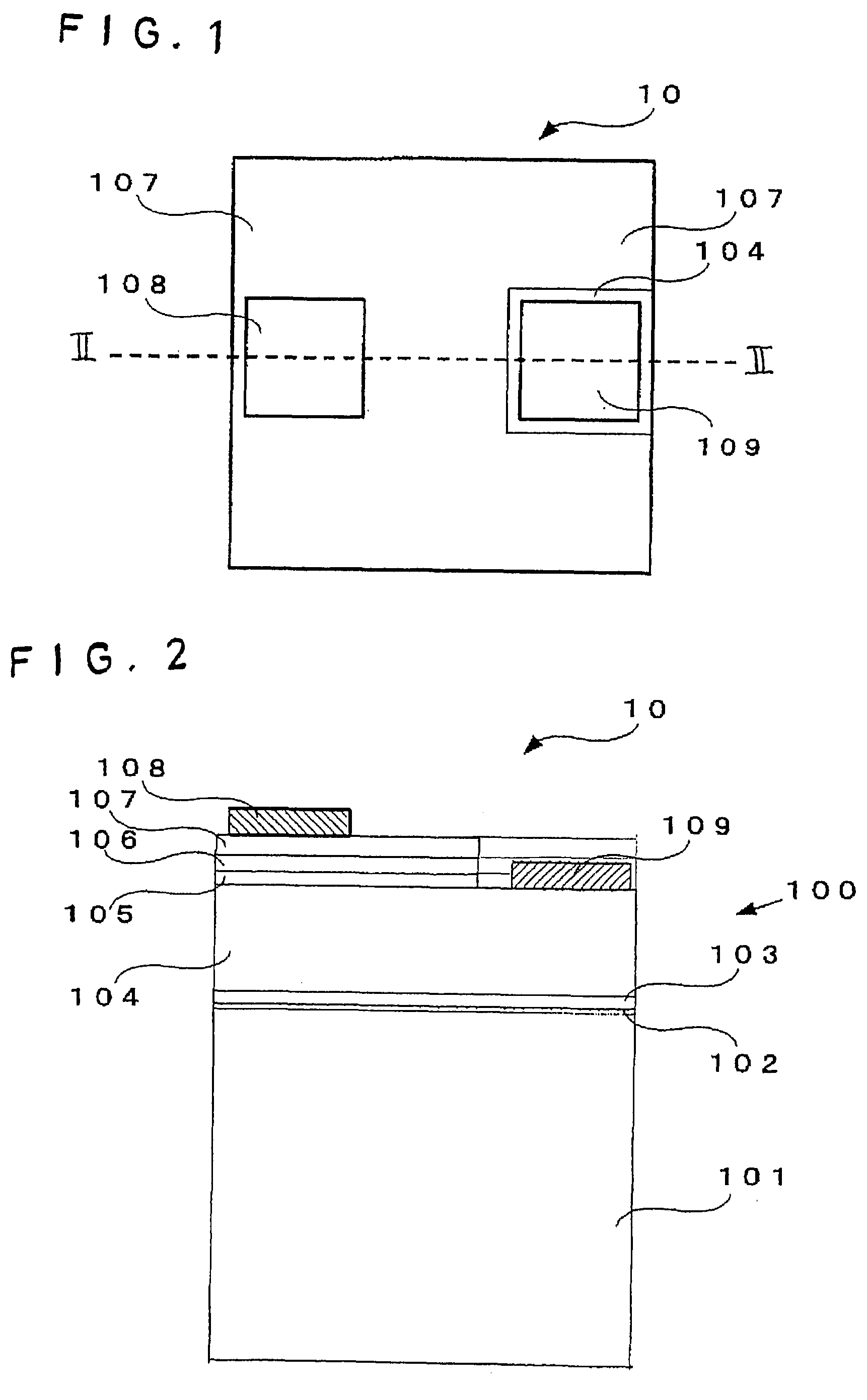
[0071]FIG. 1 illustrates a schematic planar structure of the light-emitting diode (LED) described in Example 3 and FIG. 2 a schematic sectional structure thereof taken through FIG. 1 along broken line II-II.

[0072]A stacked structure 100 for use in an LED 10 was composed by stacking a cubic (001) silicon carbide layer 102 disposed on the surface of a phosphorus (P)-doped n-type silicon single crystal substrate 101, a cubic GaN layer 103 disposed thereon, a lower clad layer 104 formed of an n-type cubic GaN doped with silicon (Si) by the MBE method, a multiple quantum well structure light-emitting layer 105 formed of a structure resulting from alternately stacking an n-type gallium-indium nitride (Ga0.9In0.1N) mixed crystal layer an...


PUM

PropertyMeasurementUnit
pressureaaaaaaaaaa
lattice constantaaaaaaaaaa

Abstract

A semiconductor layer containing defects only in a small density, possessing good quality and exhibiting a large ionic bonding property as to GaN, for example, is formed on a semiconductor layer, such as a silicon carbide layer, which is made of a material possessing a small ionicity and exhibiting a strong covalent bonding property. A method for forming a semiconductor layer includes forming on the surface of a first semiconductor layer 102 possessing a first ionicity a second semiconductor layer 103 possessing a second ionicity larger than the first ionicity. The second semiconductor layer 103 is formed while irradiating the surface of the first semiconductor layer existing on the side for forming the second semiconductor layer with electrons in a vacuum.

Description

CROSS REFERENCE TO RELATED APPLICATIONS[0001]This application is an application filed under 35 U.S.C. §111(a) claiming the benefit pursuant to 35 U.S.C. §119(e)(1) of the filing dates of Provisional Application No. 60 / 715,155 filed Sep. 9, 2005 and Japanese Patent Application No. 2005-254631 filed Sep. 2, 2005 pursuant to 35 U.S.C. §111(b).TECHNICAL FIELD[0002]This invention relates to a method for forming a semiconductor layer comprising forming on the surface of a first semiconductor layer having a first ionicity, a second semiconductor layer having a second ionicity larger than the first ionicity and to a light-emitting diode obtained using the method.BACKGROUND ART[0003]Heretofore, the technical means to form a silicon carbide layer or a gallium nitride (GaN)-based semiconductor layer on a substrate of silicon (Si), silicon carbide (SiC) or the like that excels in electrical conductivity or thermal conductivity has been known (refer to “Silicon-based Hetero Devices,” written by ...

Claims


Application Information

Patent Timeline
Patent Type & Authority Applications(United States)
IPC IPC(8): H01L21/20H01L33/00
CPCC30B23/02C30B23/025C30B29/403C30B29/406H01L21/02381H01L33/007H01L21/02461H01L21/0254H01L21/0262H01L33/005H01L21/02447
Inventor UDAGAWA, TAKASHI
Owner SHOWA DENKO KK
Why Eureka
Try Eureka