Semiconductor signal processing device

a signal processing and semiconductor technology, applied in semiconductor devices, digital storage, instruments, etc., can solve the problems of inability to achieve the performance required in current multi-media processing, direct restriction of implementable logic functions by memory capacity, and increase in cost, so as to achieve small occupation area and high speed

Inactive Publication Date: 2009-08-20
RENESAS ELECTRONICS CORP
View PDF5 Cites 112 Cited by
  • Summary
  • Abstract
  • Description
  • Claims
  • Application Information

AI Technical Summary

Benefits of technology

[0037]An object of the present invention is to provide a semiconductor signal processing device having a small occupation area, in which the operational processing can be performed at high speed even in the low power supply voltage.

Problems solved by technology

In conventional software-based processing with CPU (Central Processing Unit) and DSP (Digital Signal Processor), a performance required in current multi-media processing cannot be achieved.
However, as miniaturization of the semiconductor manufacturing process and complexity of system advance, such problems are caused as cost increase of semiconductor process, and prolonged design and verification periods and resultant cost increase.
However, in the conventional LUT operational processing unit, the implementable logic function is directly restricted by the memory capacity.
The operation cycle cannot be shortened due to the restoring, and the high-speed processing is hardly realized.
In the configuration disclosed in Japanese Patent Laying-Open No. 2007-213747, although one ferroelectric capacitor and two transfer gates are used as one operator cell, the data stored in the ferroelectric capacitor is destructively read during the operation.
Accordingly, the operational processing cannot be performed by combining different operation data with the same data.
Therefore, in order to move the sufficient amount of charges, the capacitor needs to have a significant size, which becomes an obstacle against a high integration.
Therefore, the large-capacity memory array is hardly realized in the small occupation area, and the configuration of Japanese Patent Laying-Open Nos. 07-249290 and 07-182874 is difficult to apply to the application in which a large amount of data are processed in a mobile equipment.
However, the data is destructively read in the DRAM cell.
In the configuration disclosed in Japanese Patent Laying-Open No. 2000-284943, when the logic operational circuit is provided for each pair of bit lines, it is difficult to implement a large-capacity memory array in a small occupation area.
Accordingly, in the voltage sensing type sense amplifier, because the sensing operation is slower than that of a current sensing type sense amplifier, the operation result cannot be produced at high speed, and it is difficult to implement a high-speed operation processing.
Accordingly, where an operational processing is performed by moving the charges through the use of the capacitor, the sufficient amount of charges cannot be moved at a low power supply voltage, which results in a problem that the correct operational processing cannot be ensured.
Therefore, the digital arithmetic operation cannot be performed at high speed.

Method used


Image

  • Semiconductor signal processing device
  • Semiconductor signal processing device
  • Semiconductor signal processing device

Examples


second embodiment

[0402]FIG. 25 schematically shows a configuration of a one-bit adder in a semiconductor signal processing device according to a second embodiment of the present invention. FIG. 25 shows the configuration of data path unit blocks DPUB0 to DPUB3 included in data path operation unit group (44). In the configuration of FIG. 25, a word gate circuit 100 is provided for unit operator cells UOE0 and UOE1, and a word gate circuit 102 is provided for unit operator cells UOE2 and UOE3. Unit operator cells UOE0 to UOE3 are arranged corresponding to data path unit blocks DPUB0 to DPUB3.

[0403]When an input carry Cin is “0”, word gate circuit 100 transmits the signals on write word line WWL and read word line pair RWLA / B of to a local word line group LWLG0. When input carry Cin is “1”, word gate circuit 100 maintains local word line group LWLG0 in the non-selected state.

[0404]Read word line pair RWLA / B includes read word lines RWLA and RWLB. Local word line group LWLG0 includes a local write word ...

third embodiment

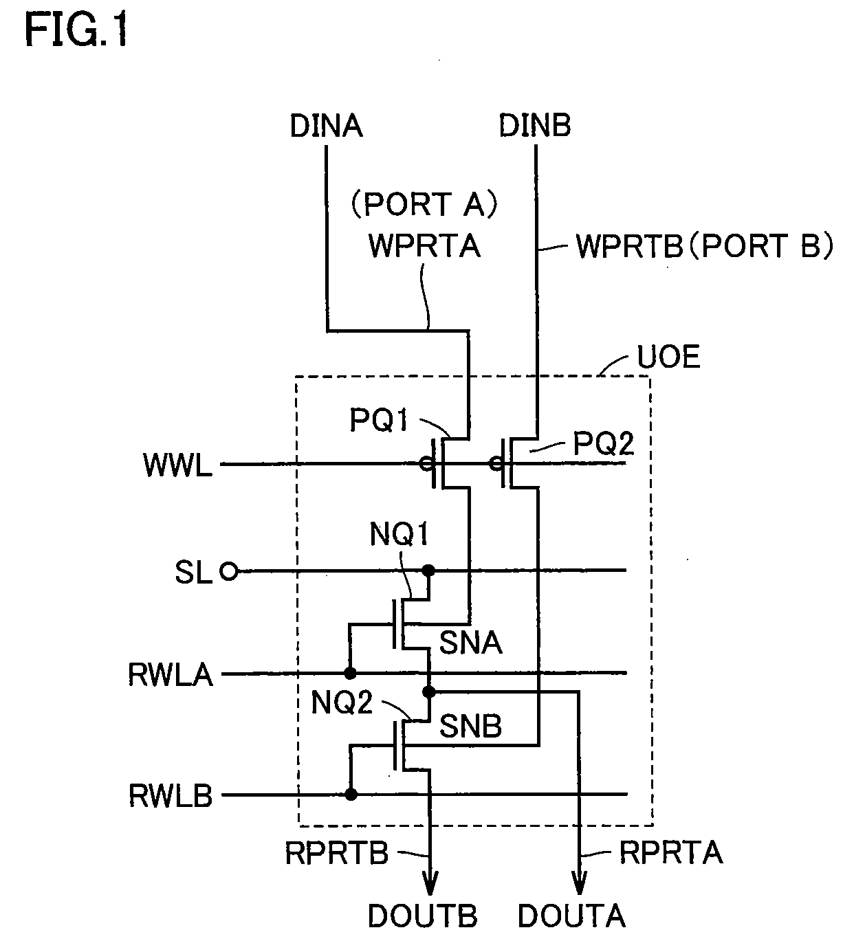
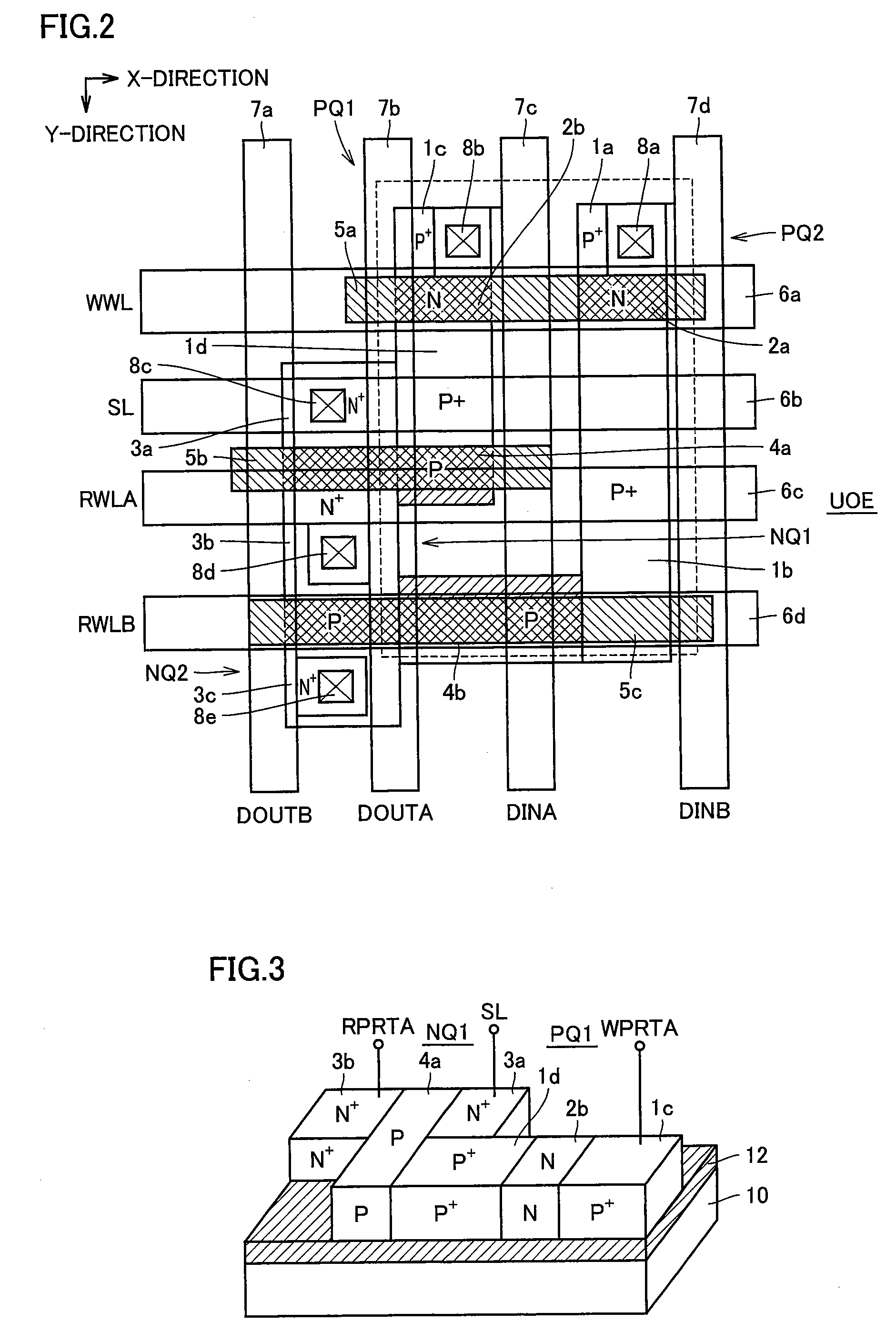
[0521]FIG. 39 shows an electrically equivalent circuit of a unit operator cell according to a third embodiment of the present invention. Unit operator cell UOE shown in FIG. 39 differs from the unit operator cell shown in FIG. 1 in that different write word lines WWLA and WWLB are provided for P-channel SOI transistors PQ1 and PQ2. In FIG. 39, because other configuration of unit operator cell UOE are similar to that of the unit operator cell shown in FIG. 1, counterparts to the unit operator cell shown in FIG. 1 are designated by the same symbols, and the detailed description is not repeated.

[0522]Where unit operator cell UOE shown in FIG. 39 is used, write word lines WWLA and WWLB can alternately be driven to the selected state, and data can be individually written in storage nodes SNA and SNB. Accordingly, with data being retained in storage node SNA, search data can be written in storage node SNB, and match / mismatch can be determined between the search data and the data stored in...

fourth embodiment

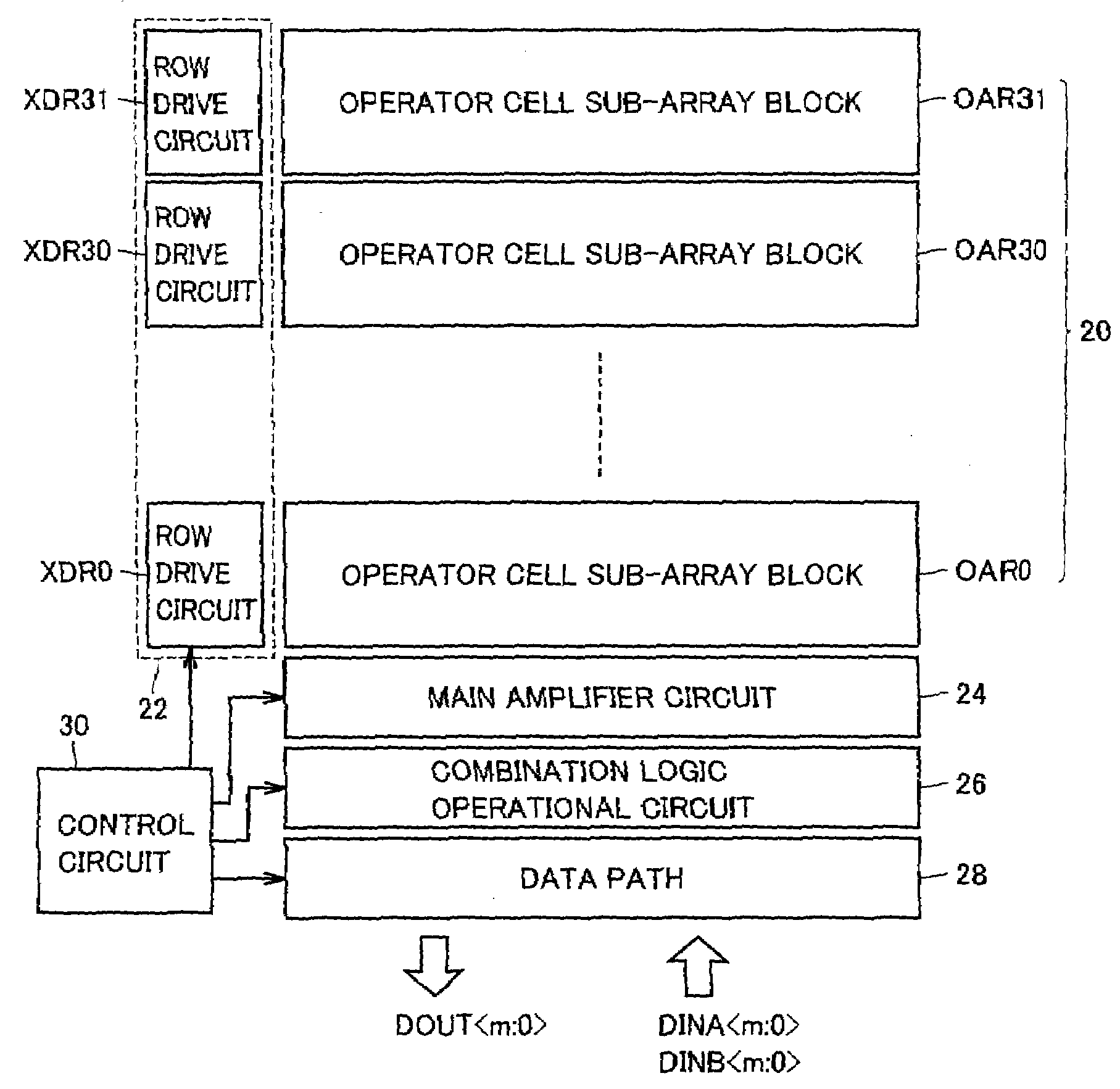
[0567]FIG. 46 schematically shows an arrangement of operational data in a semiconductor signal processing device according to a fourth embodiment of the present invention. Referring to FIG. 46, an operation data input and output processing circuit 300 is provided for operator cell array 20. Operation data input and output processing circuit 300 includes main amplifier circuit 24, combination logic operational circuit 26, and data path 28.

[0568]Operation data input and output processing circuit 300 is divided into operation unit blocks 302a, 302b, . . . . Each of operation unit blocks 302a, 302b, . . . includes unit operation block (UCL) and data path operation unit group (44) of the combination logic operational circuit.

[0569]Data words A, B, C, and D are supplied to operation data input and output processing circuit 300 in a bit serial fashion, and resultant data DOUT of operational processing (*) of the data is supplied externally in the bit serial manner. FIG. 46 shows an example...


PUM


Abstract

A unit operator cell includes a plurality of SOI (Silicon on Insulator) transistors, write data is stored in a body region of at least two SOI transistors, and the storage SOI transistors are connected in series with each other to a read port or each of the storage SOI transistors is singly connected to the read port. Therefore, an AND operation result or a NOT operation result of data stored in the unit operator cells can be obtained, and operation processing can be performed only by writing and reading data. A semiconductor signal processing device that can perform logic operation processing and arithmetic operation processing at high speed is implemented with low power consumption and a small occupation area.

Description

BACKGROUND OF THE INVENTION[0001]1. Field of the Invention[0002]The present invention relates to a semiconductor signal processing device, and particularly to a configuration of a semiconductor signal processing device including an operational circuit in which a semiconductor memory is used.[0003]2. Description of the Background Art[0004]A system LSI (Large Scale Integration) called SoC (System on Chip) is widely used to achieve down-sizing, weight-lighting and speed-up of a processing system. In SoC, a memory and a logic (processing device) are integrated on a common semiconductor substrate. In the system LSI, because the memory and the logic are connected by on-chip interconnections, a large amount of data can be transferred at high speed to allow the high-speed processing. In an article by K. Arimoto et, al., titled “A Configurable Enhanced T2RAM Macro for System-Level Power Management Unified Memory,” 2006 Symposium on VLSI Circuits, Digest of Technical Papers, June 2006 (herein...

Claims


Application Information

Patent Timeline
Patent Type & Authority Applications(United States)
IPC IPC(8): G11C5/06G11C7/00G11C11/416G11C8/00
CPCG11C8/04G11C8/12G11C11/16G11C11/405G11C11/4076H01L27/1203G11C15/02G11C15/046G11C2211/4016H01L27/0207G11C11/5607G11C11/1675
Inventor SHIMANO, HIROKIARIMOTO, KAZUTAMI
Owner RENESAS ELECTRONICS CORP
Why Eureka
Try Eureka