Colloidal silica for semiconductor wafer polishing and production method thereof

Inactive Publication Date: 2009-10-29
NIPPON CHECMICAL IND CO LTD +1
View PDF6 Cites 22 Cited by
  • Summary
  • Abstract
  • Description
  • Claims
  • Application Information

AI Technical Summary

Benefits of technology

[0030]By using a colloidal silica for polishing of the present invention, one can obtain excellent effect in preventing over etching in polishing of a semiconductor wafer and the like. “Over etching” is a phenomenon that causes by corrosion of a wiring metal which results formation of recesses during polishing process of the wiring metal, an insulation film or a barrier film. Over etching occurs when a balance of corrosive speed between a mechanical polishing action by polishing particles and a corrosive action by alkaline component is broken. Over etching is recognized a

Problems solved by technology

If outermost periphery edge of the wafer is unevenly structured at the transportation, minute crushes are caused at the edge part of the wafer when the wafer collides with a transporting device and fine particles arose.
The fine particles arisen scatter and contaminate the precisely processed wafer surface, and affect seriously on yield and quality of products.
Especially, amines claim attention as an agent that seldom over etches a wafer, however, a problem has n

Method used


Image

  • Colloidal silica for semiconductor wafer polishing and production method thereof
  • Colloidal silica for semiconductor wafer polishing and production method thereof
  • Colloidal silica for semiconductor wafer polishing and production method thereof

Examples


Example

Example 1

[0077]Hydrolysis of tetrametoxysilane is practiced by a composition of 4.49 mol / L tetrametoxysilane, 0.01 mol / L acid, and 18.38 mol / L water without using solvent. Practically, hydrolysis is performed by processes mentioned below.

[0078]Diluted hydrochloric acid solution is prepared by adding 0.2 g of 35% hydrochloric acid into 46 g of deionized water. 96 g of tetrametoxysilane (special grade reagent, converted SiO2 concentration is 39 wt %) is placed into a container, then above mentioned diluted hydrochloric acid solution is added with stirring. At the first stage, said two solutions are separated and are not mixed well. After several minutes, hydrolysis reaction starts with heat evolution, and the mixture becomes transparent homogeneous solution. Stirring is continued another 30 minutes so as the hydrolysis reaction to be completed, and hydrolyzed solution is obtained. Then said solution is diluted by adding 116 g of deionized water to prevent the polymerization of active ...

Example

Example 2

[0082]By same method as Example 1, tetramethoxysilane is hydrolyzed and an active silicic acid aqueous solution having SiO2 concentration of 3.7 wt % and a pH of 2.6 is obtained. The pH is adjusted to 9.8 by adding 64 g of a 10% morpholine aqueous solution to 500 g of the active silicic acid aqueous solution with stirring. After that, solutions are heated with stirring, maintained at 100° C. for 1 hour, to form colloid particles. Then, while maintaining the temperature at 100° C., 2600 g of the active silicic acid aqueous solution and 40 g of the 10% morpholine aqueous solution are simultaneously added by 4 hours to grow silica particles. After adding process, the solution is matured by maintaining the temperature at 100° C. for 1 hour, then cooled down.

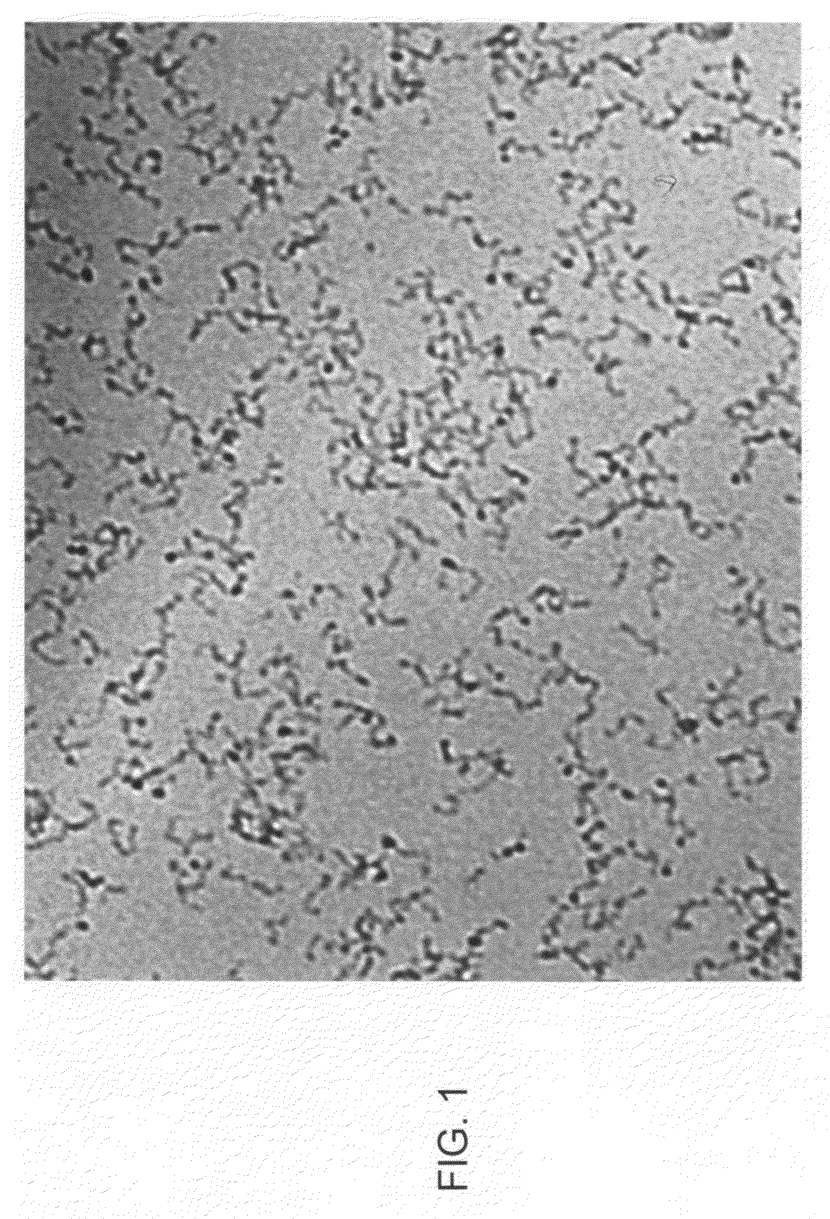
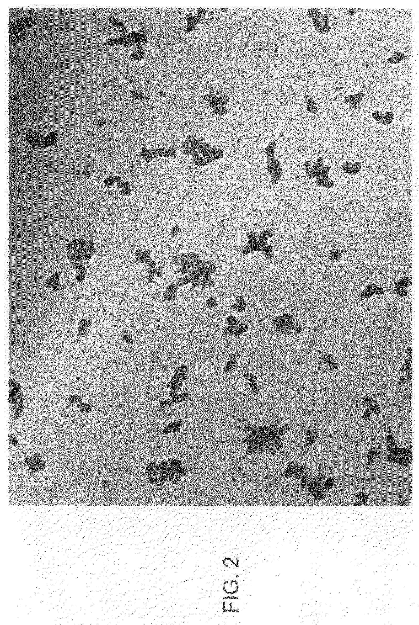
[0083]Silica concentration of obtained colloidal silica becomes 5.6 wt % due to evaporation of water and a pH at 25° C is 9.0. According to a transmission electron microscope (TEM) observation, obtained colloidal silica is c...

Example

Example 3

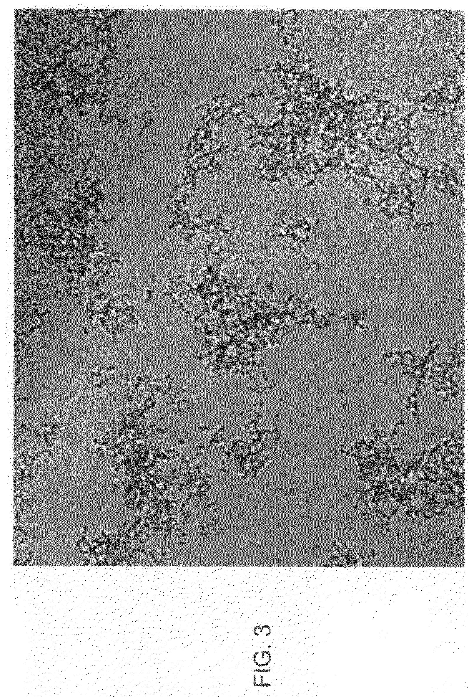
[0084]Colloidal silica obtained by Example 2 is concentrated. After that, pressure filtration by pump circulation is carried out using hollow fiber ultra-filter membrane whose molecular cutoff value is 6000 (MICROZA UF MODULE SIP-1013, product of ASAHI KASEI Corp.). In this way, colloidal silica is concentrated to make the solution having SiO2 concentration of 22.1 wt % and approximately 520 g of concentrated colloidal silica is obtained. Obtained colloidal silica has a pH of 8.6 at 25° C., and alkali metal concentration is smaller than 1 ppm.


PUM


Abstract

Colloidal silica forming nonspherical particles cluster, whose long axis/short axis ratio of silica particles is of 1.2 to 20, and average long axis/short axis ratio of 3 to 15. This colloidal silica can be produced by forming particles by adding basic nitrogen compounds to an active silicic acid aqueous solution, the solution which produced by hydrolysis of tetraalkoxysilane, while heating, then growing particles by using a build up method.

Description

FIELD OF THE INVENTION[0001]The present invention relates to colloidal silica for semiconductor wafer polishing that polishes a surface or an edge part of a semiconductor wafer such as a silicon wafer or a semiconductor device substrate with a film such as a metal film, an oxide film, a nitride film or the like (hereinafter shortened to metal films) on the surface, and the production method thereof.[0002]Hereinafter, “colloidal silica for semiconductor wafer polishing” can be shortened to “colloidal silica for polishing”.BACKGROUND OF THE INVENTION[0003]Electronic components such as ICs, LSIs or ULSIs which applying semiconductor materials, such as silicon single crystal, as raw material can be manufactured based on a small semiconductor device chips. Said small semiconductor device chips are fabricated by dicing thin disk shaped wafers on which a number of fine electronic circuits are built to semiconductor chips, where the wafers are fabricated by slicing a single crystal ingot of...

Claims


Application Information

Patent Timeline
IPC IPC(8): C09K13/00B24B37/00B82Y10/00B82Y30/00B82Y99/00C01B33/151C09K3/14H01L21/304
CPCC09K3/1463
Inventor NAKAJO, MASARUSAITO, YUKIYOOHKUBO, KUNIOMAEJIMA, KUNIAKITANAKA, HIROAKI
Owner NIPPON CHECMICAL IND CO LTD
Why Eureka
Try Eureka