Semiconductor device including capacitorless ram

Active Publication Date: 2009-12-17
LONGITUDE LICENSING LTD
View PDF9 Cites 55 Cited by
  • Summary
  • Abstract
  • Description
  • Claims
  • Application Information

AI Technical Summary

Benefits of technology

[0009]wherein: the field effect transistor includes a first region comprising a first semiconductor having a given band gap and a second region comprising a second semiconductor having a larger band gap than the first semiconductor; and
[0010]a channel body region of the field effect transistor is disposed in the first region comprising the first semiconductor.
[0011]According to another embodiment of the present invention, there is provided a semiconductor device in which: the field effect transistor comprises the channel body region; a source region; a drain region; and a contact region electrically connected to said source or said drain region; and the second region comprising said second semiconductor is disposed between the channel body region and the contact region.
[0012]In the FBC type capacitorless RAM (hereinafter, referred to as an FBC type RAM) according to the present embodiment, the channel body region acting as floating body includes the first semiconductor having a given band gap, and the second semiconductor having a larger band gap than at least the first semiconductor is arranged between the con

Problems solved by technology

In order to achieve a high degree of integration, the footprint of individual capacitors has been increasingly miniaturized, so a configuration of a high aspect ratio is used to provide a required capacitance, making the fabrication thereof more difficult.
However, according to the related art, the f

Method used


Image

  • Semiconductor device including capacitorless ram
  • Semiconductor device including capacitorless ram
  • Semiconductor device including capacitorless ram

Examples


Example

First Embodiment

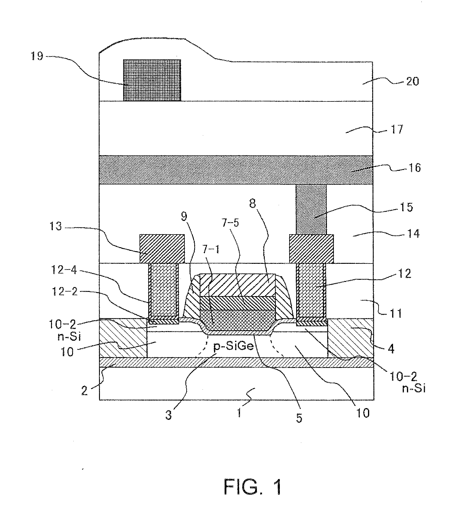
[0043]FIG. 1 illustrates a structure of the main part of an n-type MOS floating body cell (FBC) surrounded by an insulating film according to a first embodiment of the present invention. The main part includes, on semiconductor substrate 1, buried insulating film 2, body region 3, element isolation insulating film 4, gate insulating film 5, gate electrode 7 (gate polycrystalline silicon 7-1, gate metal layer 7-5), cap insulating film 8, sidewall spacer 9, source and drain region 10, insulating film (1) 11, contact plug 12, line (M1) 13, insulating film (2) 14, via plug (1) 15, bit line 16, insulating film (2) 17, line (M3) 19 and protective insulating film 20. Here, body region 3 includes p-type SiGe being a first semiconductor and has a smaller band gap than n-type Si being a second semiconductor constituting source and drain region 10.

[0044]Body region 3 is isolated from semiconductor substrate 1 by use of buried insulating film 2, and also electrically isolated fr...

Example

Second Embodiment

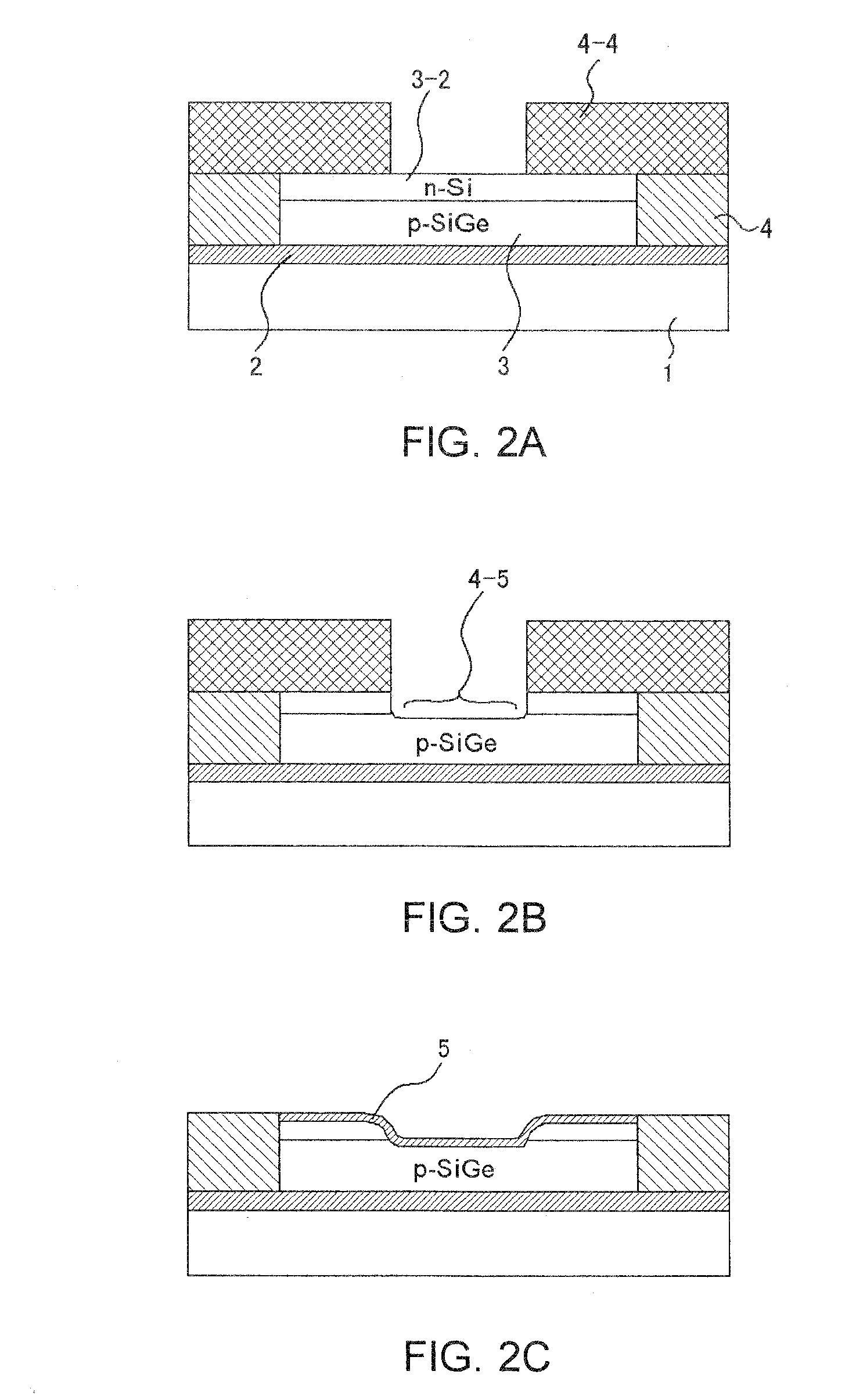
[0054]A variation (second embodiment) is illustrated in FIGS. 3A to 3E.

[0055]An SOI substrate having buried insulating film 2 formed on substrate 1 is used. P-type SiGe is used for a semiconductor layer (body region 3) on buried insulating film 2. Element isolation insulating film 4, gate insulating film 5, polycrystalline silicon 7-1, metal layer 7-5 and cap insulating film 8 are sequentially formed and after processing the materials, gate electrode 7 is formed.

[0056]Here, a silicon oxide film or silicon oxynitride film containing nitrogen may be used for gate insulating film 5. Silicon oxynitride film has excellent resistance against exudation of dopant contained in polycrystalline silicon, so that it is preferable to use silicon oxynitride film.

[0057]Here, metal silicide such as silicides of refractory metal (e.g., tungsten silicide, titanium silicide or cobalt silicide) may also be used for metal layer 7-5. Alternatively, when metal layer 7-5 is constructed as a...

Example

Third Embodiment

[0060]Another variation (third embodiment) will be described. FIG. 4A illustrates a cross-sectional structure of a transistor of a floating body structure having polycrystalline silicon 6-1 formed therein. This polycrystalline silicon 6-1 is a dummy gate, and semiconductor layer 3-1 is composed of p-type Si, but in other aspects, the same reference numerals are applied to parts corresponding to those of the above described embodiment. Subsequently, smoothed insulating film 11 is formed (FIG. 4B), and polycrystalline silicon 6-1 being a dummy gate is etched and removed.

[0061]Subsequently, p-type Si semiconductor layer (3-1) is doped with Ge via part (6-2) obtained by removing the dummy gate, whereby Ge-doped p-type Si region (3-5) is formed (FIG. 4C). In this doping, ion implantation or plasma doping technique may be used. The damaged oxide film is removed, the surface of the substrate is cleaned and thereafter gate insulating film 5 is formed. Then, a gate electrode ...


PUM


Abstract

There is provided a semiconductor device including a capacitorless RAM. The semiconductor device includes a field effect transistor (FET) having a floating body structure. FET includes a channel body region arranged in a first region comprising a first semiconductor (e.g., p-SiGe) having a given band gap and a second region comprising a second semiconductor (e.g., n-Si) having a larger band gap than the first semiconductor.

Description

BACKGROUND OF THE INVENTION[0001]1. Field of the Invention[0002]The present invention relates to a semiconductor device, and more particularly to a floating body cell (hereinafter referred to as “FBC”) type capacitorless RAM (Random Access Memory) which is electrically isolated from a substrate by use of an insulating material.[0003]2. Description of the Related Art[0004]In conventional DRAMs, electric charges are accumulated in capacitors to store information. In order to achieve a high degree of integration, the footprint of individual capacitors has been increasingly miniaturized, so a configuration of a high aspect ratio is used to provide a required capacitance, making the fabrication thereof more difficult. In order to address this problem, a cell (FBC) has been proposed which stores information using the floating body effect of transistor without using a capacitor. For example, FBC type RAM has been described in U.S. Pat. No. 6,969,662, National Publication of International P...

Claims


Application Information

Patent Timeline
IPC IPC(8): G11C7/02H01L29/66
CPCG11C7/067G11C11/404G11C11/4091H01L29/7841G11C2211/4016H01L27/108H01L27/10802G11C2207/005H10B12/20H10B12/00
Inventor SAITO, MASAYOSHI
Owner LONGITUDE LICENSING LTD
Why Eureka
Try Eureka