

GHz Surface Acoustic Resonators in RF-CMOS
a surface acoustic wave and cmos technology, applied in piezoelectric/electrostrictive transducers, instruments, transducer types, etc., can solve the problems of inability to hybridize or integrate into sensing chip technology, poor rf performance of cmos devices, and low sensitivity, so as to improve the arrangement performance of biosensors and the effect of rapid detection and quantification of analytes
- Summary
- Abstract
- Description
- Claims
- Application Information
AI Technical Summary
Benefits of technology
Problems solved by technology
Method used
Image

Examples
examples
[0158]In these example implementations, one deposition step is eliminated since standard CMOS metal layers are used to implement the transducers' structures. The maturity and precision of the standard 0.6 μm CMOS technology enables us to manufacture very well-defined metal features to implement the transducers, with minimum widths of 0.9 μm, resulting in very high frequency resonators of 1.02 GHz.
[0159]These examples present the design, fabrication, equivalent circuit model and characterization measurements of three two- port resonators.
example i
[0160]The design of the CMOS SAW resonators is described first, where the key design factors that affect the resonant frequency and quality factor are highlighted. Next, the fabrication sequence of implementing the surface acoustic wave resonators in CMOS with three additional post- processing steps is illustrated in detail. Characterization of the piezoelectric zinc oxide layer using x-ray diffraction, scanning electron microscopy (SEM) and atomic force microscopy is also reported. The fabricated resonators were measured to obtain its S21 and S11 transmission and reflection characteristics. To verify the resonant frequency of the device, finite element modeling of the device was also done using CoventorWare®. Based on the measurement results and the fabrication layers of the CMOS resonators, an equivalent circuit model specifically for two-port CMOS surface acoustic wave resonators was developed. Simulations using the developed equivalent circuit were compared with the experimental...
example — ii
Example—II
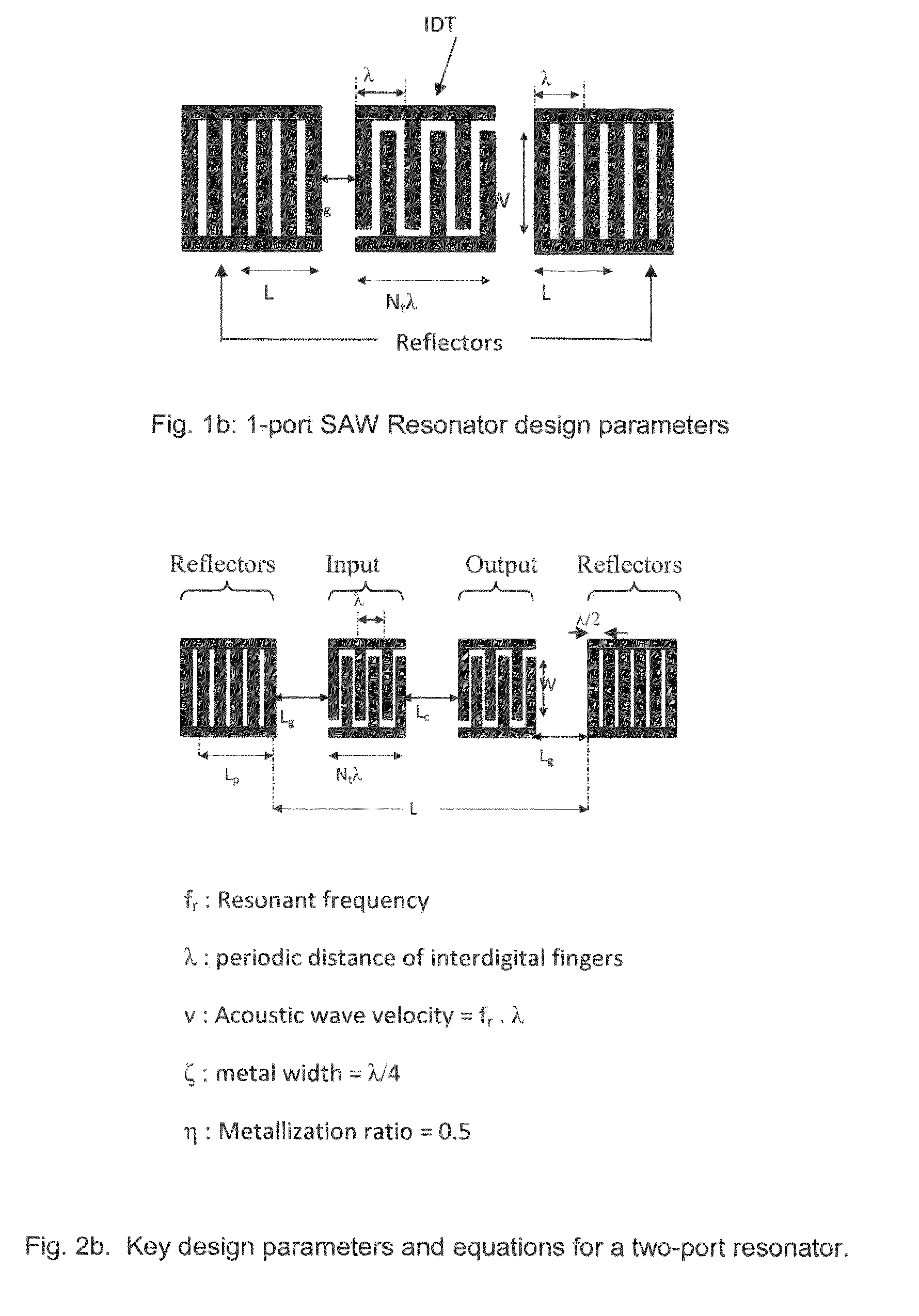
Resonator Design
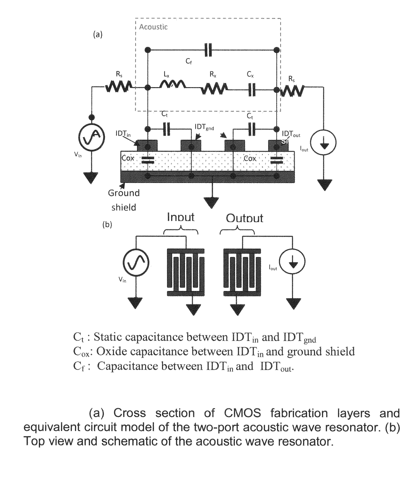
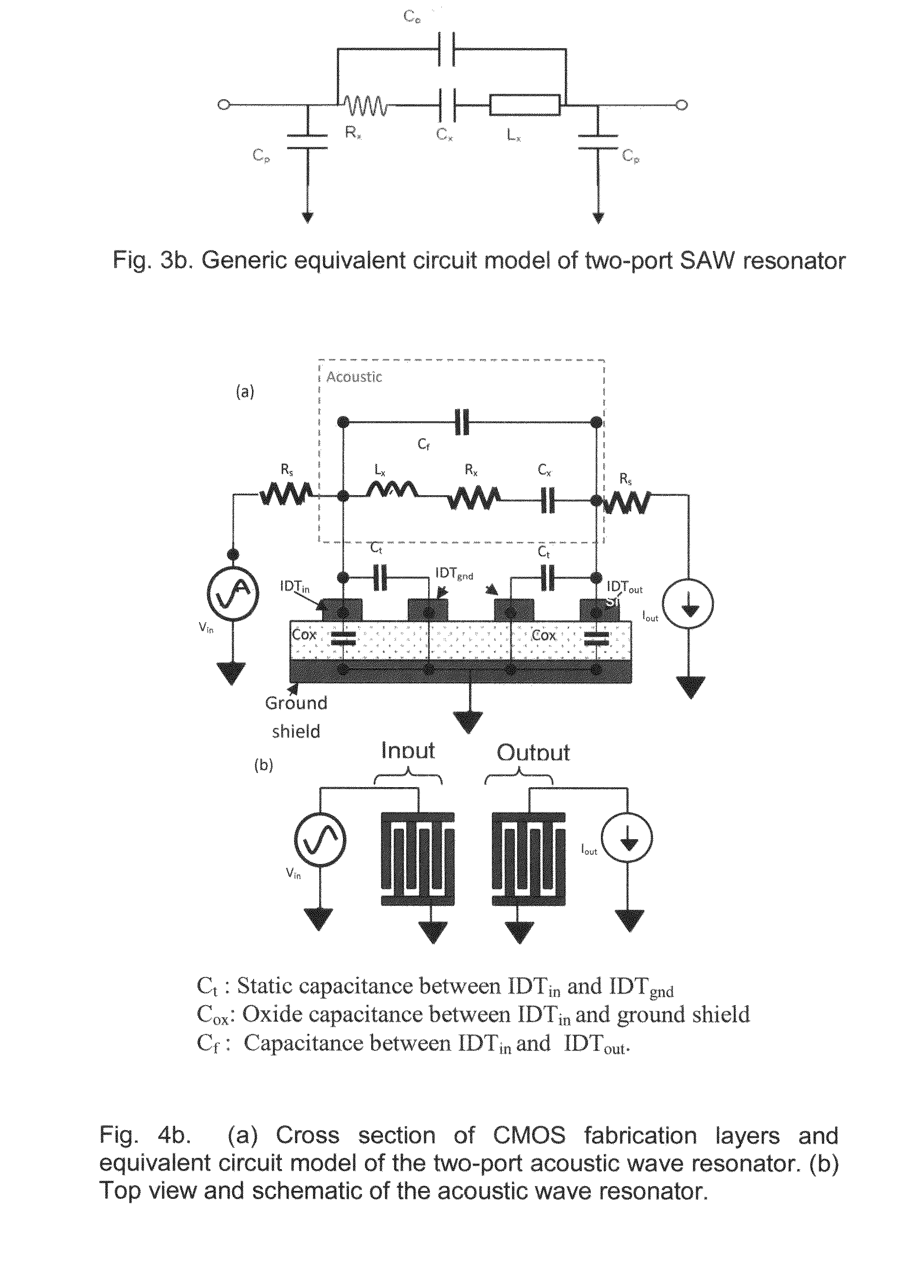
[0161]A. Resonator Structure
[0162]The structure of a two-port CMOS SAW resonator consists of input and output interdigital transducers, which are flanked by a bank of shorted reflectors on each side. Shorted reflectors have been shown to have less spurious effects compared to unconnected reflectors and have been used in all our designs.
[0163]When a sinusoidal signal is injected at the input port, acoustic waves propagating in both directions are generated in the piezoelectric zinc oxide layer. The acoustic waves are detected and translated back into an electrical signal at the output port. The reflectors minimize the losses by containing the acoustic waves within the cavity, to create standing waves or resonance.
[0164]FIG. 6(b) (a) illustrates the cross-section of the CMOS resonator implemented for design 1 and design 2. This implementation utilized two CMOS metal layers, namely metal 1 for the ground shield and metal 2 for the reflectors and transducers. I...
PUM
| Property | Measurement | Unit |
|---|---|---|
| Length | aaaaa | aaaaa |
| Length | aaaaa | aaaaa |
| Length | aaaaa | aaaaa |
Abstract
Description
Claims
Application Information