Engineered oxygen profile in metal gate electrode and nitrided high-k gate dielectrics structure for high performance pmos devices

a technology of dielectric structure and metal gate electrode, which is applied in the direction of transistors, electrical devices, semiconductor devices, etc., can solve the problems of less performance than desired from metal gate pmos transistors, and achieve the effects of reducing the threshold increase of pmos transistors, reducing oxygen diffusion, and reducing gate depletion effects

Active Publication Date: 2010-03-04
TEXAS INSTR INC
View PDF3 Cites 41 Cited by
  • Summary
  • Abstract
  • Description
  • Claims
  • Application Information

AI Technical Summary

Benefits of technology

[0004]The instant invention provides a p-channel metal-oxide-semiconductor (PMOS) transistor which includes a nitrogen containing barrier to oxygen diffusion between a gate dielectric layer and a metal gate in the PMOS transistor, in combination with a low oxygen region of the metal gate, with a work function above 5 electron volts, and with an oxygen content below 2 percent, and preferably below 1 percent, in contact with the nitrogen containing barrier and an oxygen rich region of the metal gate, also with a work function above 5 electron volts, with an oxygen content above 10 percent, and preferably above 20 percent, in contact with the low oxygen content metal region. The nitrogen containing barrier may reduce oxygen diffusion from the gate dielectric layer to the metal gate, which may reduce threshold increases in PMOS transistors with gate dielectric layers thinner than 2 nanometers. The low oxygen content metal region reduces gate depletion effects while the oxygen rich metal region desirably increases a work function of the metal gate to a value closer to p-type polycrystalline silicon (commonly known as polysilicon) doped above 1019 cm−3.
[0007]An advantage of the inventive PMOS transistor is that it is compatible with planar fabrication processes and with get replacement fabrication processes.

Problems solved by technology

Moreover, work functions of metal gates commonly do not match work functions in p-type polycrystalline silicon gate electrodes, leading to less performance than desired from metal gate PMOS transistors.

Method used


Image

  • Engineered oxygen profile in metal gate electrode and nitrided high-k gate dielectrics structure for high performance pmos devices
  • Engineered oxygen profile in metal gate electrode and nitrided high-k gate dielectrics structure for high performance pmos devices
  • Engineered oxygen profile in metal gate electrode and nitrided high-k gate dielectrics structure for high performance pmos devices

Examples


first embodiment

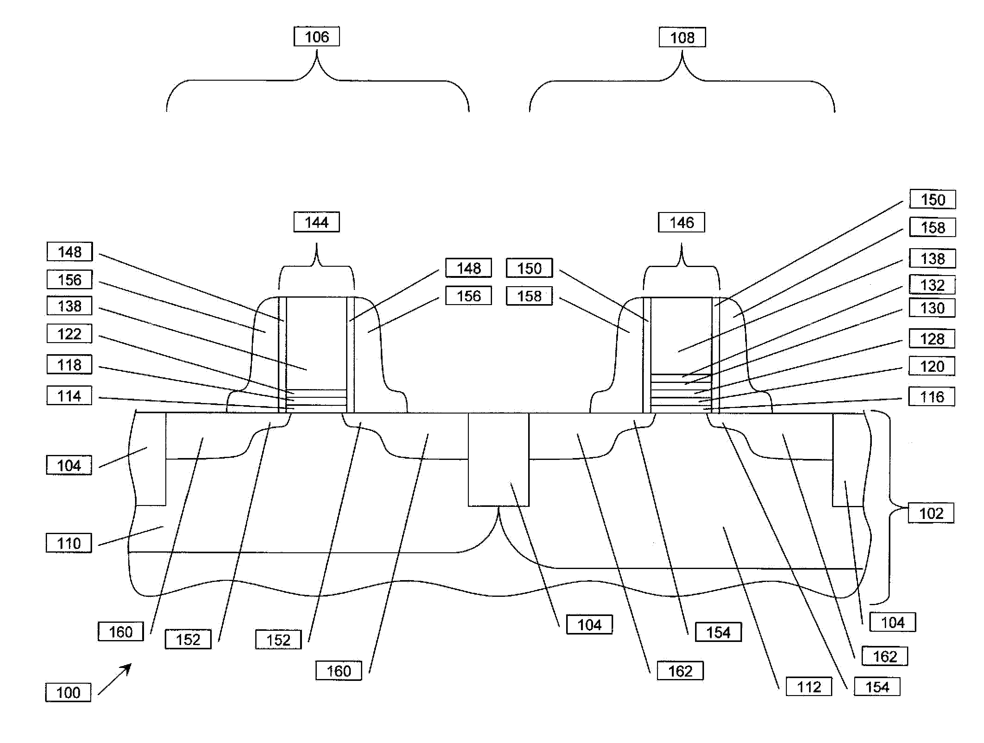
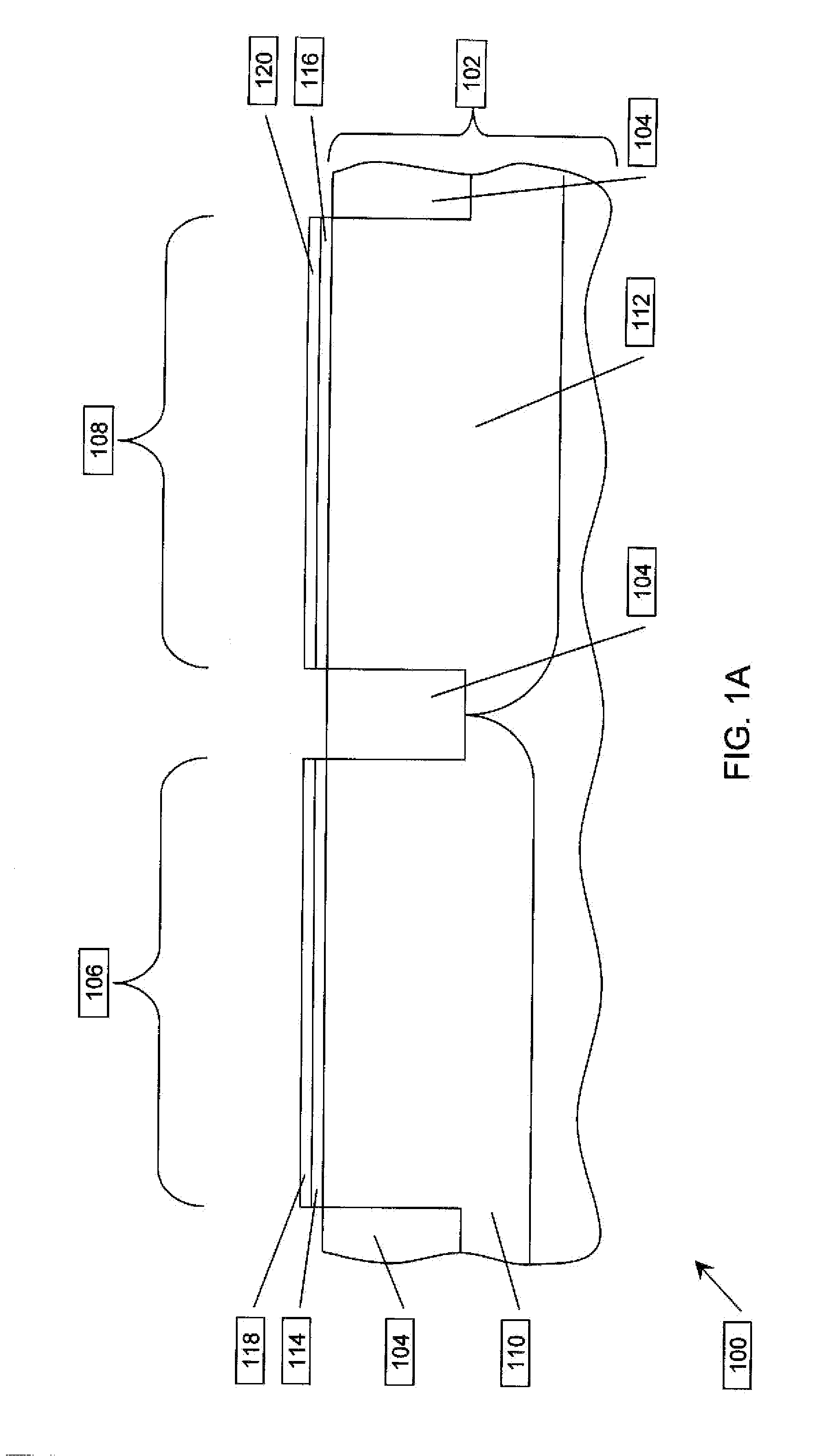
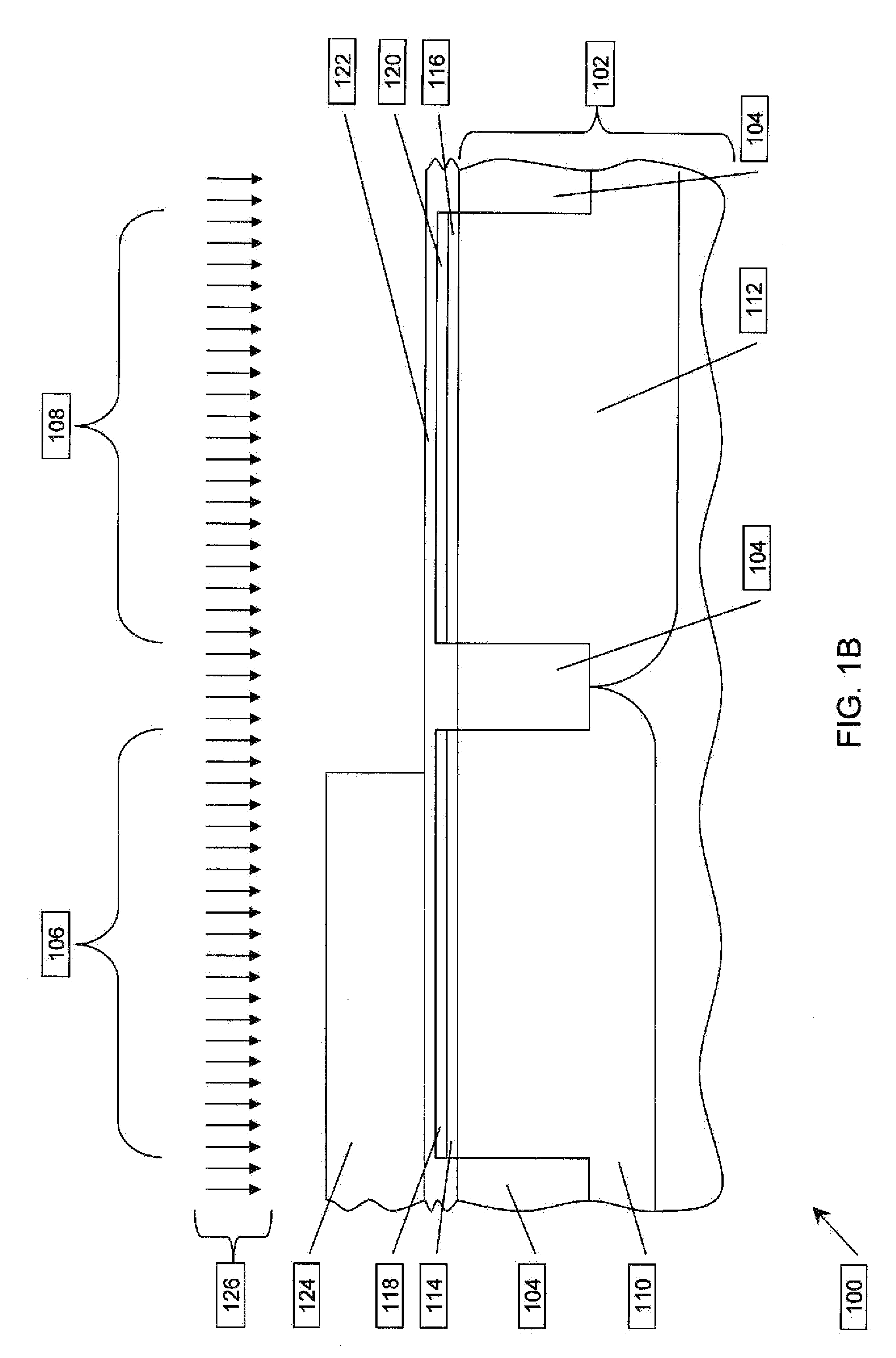
[0017]FIG. 1A through FIG. 1J are cross-sections on an IC containing the instant invention formed by a planar fabrication process sequence, depicted in successive stages of fabrication. Referring to FIG. 1A, the IC 100 is formed on a substrate 102 which is commonly a single crystal silicon wafer, but may be a silicon-on-insulator (SOI) wafer, a hybrid orientation technology (HOT) wafer with regions of different crystal orientations, or other material appropriate for fabrication of the IC 100. Elements of field isolation 104 are formed at a top surface of the substrate 102, typically of silicon dioxide between 250 and 600 nanometers thick, commonly by shallow trench isolation (STI) or local oxidation of silicon (LOCOS) processes. In STI processes, silicon dioxide may be deposited by high density plasma (HDP) or high aspect ratio process (HARP). An element of field isolation 104 separates a region in the IC 100 defined for an n-channel metal oxide semiconductor (NMOS) transistor 106 f...

second embodiment

[0032]FIG. 2A through FIG. 2H are cross-sections on an IC containing the instant invention formed by a gate replacement fabrication process sequence, depicted in successive stages of fabrication. Referring to FIG. 2A, the IC 200 is formed on a substrate 202 which has the properties described in reference to FIG. 1A. Elements of field isolation 204 are formed in the substrate 202 as described in reference to FIG. 1A. An element of field isolation 204 separates a region in the IC 200 defined for an NMOS transistor 206 from a region in the IC 200 defined for a PMOS transistor 208. A p-well 210 is formed in the substrate 202 in the NMOS region 206, as described in reference to FIG. 1A. Similarly, an n-well 212 is formed in the substrate 202 in the PMOS region 208, as described in reference to FIG. 1A. An NMOS gate dielectric layer 214 is formed on a top surface of the p-well 210, with the properties described in reference to FIG. 1A. A PMOS gate dielectric layer 216 is formed on a top s...


PUM


Abstract

A PMOS transistor is disclosed which includes a nitrogen containing barrier to oxygen diffusion between a gate dielectric layer and a metal gate in the PMOS transistor, in combination with a low oxygen region of the metal gate in direct contact with the nitrogen containing barrier and an oxygen rich region of the metal gate above the low oxygen content metal region. The nitrogen containing barrier may be formed by depositing nitrogen containing barrier material on the gate dielectric layer or by nitridating a top region of the gate dielectric layer. The oxygen rich region of the metal gate may be formed by depositing oxidized metal on the low oxygen region of the metal gate or by oxidizing a top region of the low oxygen region of the metal gate.

Description

FIELD OF THE INVENTION[0001]This invention relates to the field of integrated circuits. More particularly, this invention relates to metal gates in MOS transistors in integrated circuits.BACKGROUND OF THE INVENTION[0002]Metal gate electrodes are fabricated in metal oxide semiconductor (MOS) transistors in some advanced integrated circuits (ICs) to increase performance parameters such as on-state drive current. It is observed that p-channel metal-oxide-semiconductor (PMOS) transistors with metal gate electrodes may exhibit an increase in threshold voltages as the gate dielectric layer thicknesses decrease to ranges used in high performance complementary metal-oxide-semiconductor (CMOS) ICs, for example below 2 nanometers. Moreover, work functions of metal gates commonly do not match work functions in p-type polycrystalline silicon gate electrodes, leading to less performance than desired from metal gate PMOS transistors.SUMMARY OF THE INVENTION[0003]This Summary is provided to comply...

Claims


Application Information

Patent Timeline
Patent Type & Authority Applications(United States)
IPC IPC(8): H01L27/092H01L21/8238
CPCH01L21/28202H01L21/823842H01L29/66545H01L29/518H01L21/823864
Inventor NIIMI, HIROAKIWEN, HUANG-CHUN
Owner TEXAS INSTR INC
Why Eureka
Try Eureka