[0022]The present invention also comprises forming a filled through via and upper pad structure in the thinned and bonded substrate that rivets the substrates together and improves the
mechanical integrity of the bonded structures. The through vias of this invention comprise an
electrically conductive material such as Al, Mo, W, Cu, Au, Ag, Pd, Pt, Ni, or combinations thereof with one another, which includes alloys or mixtures thereof, or alloys or mixtures thereof with equivalent elements, or equivalent materials, compounds or alloys. The current invention also enables high
bond strength between device
layers by utilizing a suitable
adhesive layer that is compatible with the thermal budget of the device
layers being bonded together. These objects and the associated embodiments are described in detail below along with illustrative drawings listed herein.
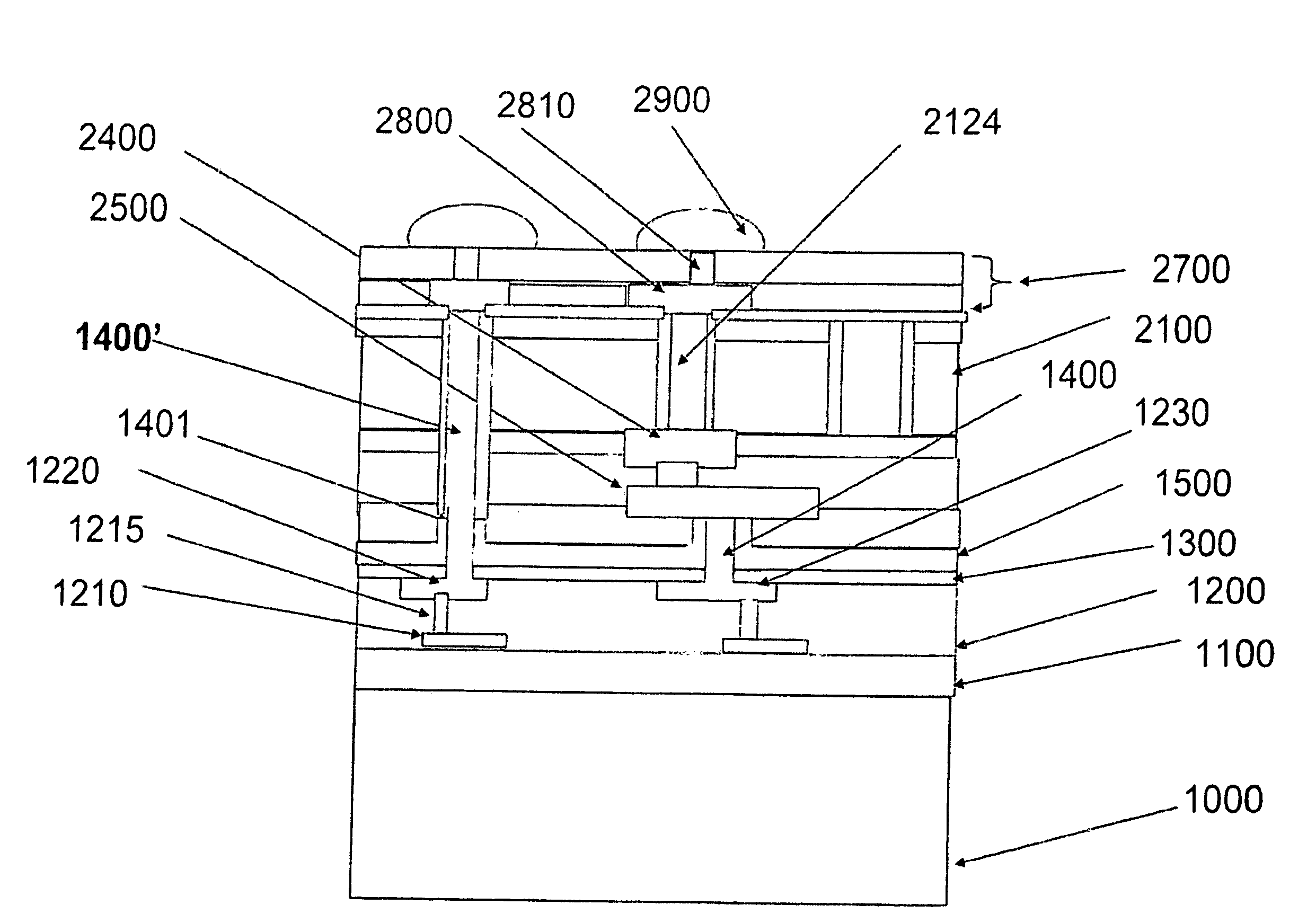
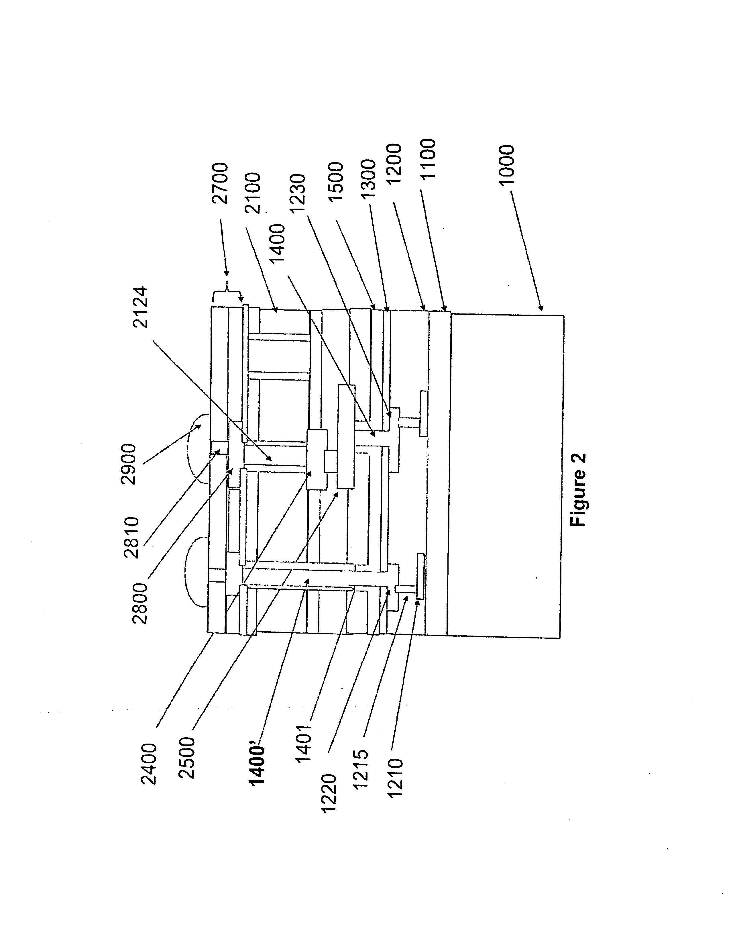
[0026]These TSV's connect to selected locations of the device in device layer 2100 and to selected points 2240 of the interconnects in the interconnect layer 2200 on this thinner device substrate. Substrate 2000 is also provided with an
insulation layer 2300 and a set of pads 2400, the pads being connected to selected locations 2250 in the interconnects in the interconnect layer 2200. Studs 1400 and pads 2400 are bonded together to enable
electrical connection between the two substrates while an
adhesive 1500 provides a mechanically robust bond between the substrates. The top of the bonded structure is also provided with additional interconnects 2700 and I / O (input / output) terminals 2900 as shown. We have previously demonstrated that T&J stud / via structures can be built between about 1 um to about 3 um in thickness for
oxide ILD. For
polyimide ILD thickness is normally 3-30 um. We also demonstrated that the entire Si bulk can be removed from the bonded wafers by a judicious combination of
wafer grinding,
polishing and RIE processes after the Si
wafer is securely bonded to a carrier wafer or a bottom device wafer.
[0032]Thus, a fundamentally important feature of the present approach is that the through via electrical continuity between the bottom and top wafer(s) is not dependent on deep Si etch and fill yields or metal to metal bonding yields as in the case of the conventional 3DI or 3DI T&J approaches. Since in the current approach, the connection between the studs in the bottom wafer and the “
rivet head” which is part of the upper wafer is achieved by the traditional metallization processes (after optionally cleaning the metal stud exposed in the through vias), this connection can be made as
high yielding and robust as a standard via connection in a BEOL build with relaxed via dimensions. This is likely to be significantly better than what one might expect for the combined deep Si etch and fill plus metal to metal bonding yields practiced in the prior art 3D integration approaches.
[0033]Another important benefit that can be derived from this through via approach is the option to print and etch standard alignment marks at the same time as when the through via recess is etched into the upper
silicon wafer. These marks will be exposed after lamination and upper
wafer thinning and appear as trench marks when viewed from the top. As such these can be used for lithographic alignment of any added patterns or additional bonding layers added on top. In the conventional 3DI approach, transfer marks required for this alignment need to be made by deep
silicon etching. Limitation in aspect ratios and RIE
lag issues dictate that these marks necessarily be coarse. Their fidelity can also be less than optimal due to the deep silicon etch needed to etch them through a large depth of silicon. In contrast, as the etch depth involved in the present inventive approach is much less and can easily accommodate the standard fine size
stepper alignment marks. This improves the ease and accuracy of alignment of post-lamination added patterns and layers to the second wafer.
[0034]Other embodiments include the use of a
passivation layer based on
passivation materials such as those comprising
silicon nitride applied to the walls of the through via recesses (by a deposition and etch method analogous to a sidewall spacer process) to insulate the inserted stud and the added metal fill after joining from the devices in the upper layer SiN
passivation can also be deposited on the studs and the surface of the bottom wafer before applying the adhesive layer in order to hermetically seal the
copper during the preparation, alignment and bonding steps. This SiN
coating can be etched off by RIE or similar process at the specific contact locations desired just before the added metal fill process is performed. Such a structure provides a further insurance against any adverse interaction of the through via metal or added metal fill with the device layers in the upper wafer and provides passivation of metal features from an environmental ingress and reliability perspective. Additionally, selective metal passivation using electroless Sn, Au or Co—W—P coatings can be performed to the studs if desired to improve their
corrosion resistance.

