Low-loss ferrite and electronic device formed by such ferrite

a technology of low-loss ferrite and electronic devices, which is applied in the direction of magnetic materials, inductances, magnetic bodies, etc., can solve the problems of reduced conversion efficiency, less ac resistance (ac resistance of conductor lines and core loss of ferrite) and less noise, and achieves low loss and small variation of characteristics.

Active Publication Date: 2010-04-08
HITACHI METALS LTD
View PDF8 Cites 36 Cited by
  • Summary
  • Abstract
  • Description
  • Claims
  • Application Information

AI Technical Summary

Benefits of technology

[0011]Accordingly, an object of the present invention is to provide ferrite sinterable at lower temperatures than the melting point of Ag, having low loss at as high a frequency as 10 MHz, and suffering little variation of characteristics under stress, and an electronic device using this ferrite.DISCLOSURE OF THE INVENTION

Problems solved by technology

Because of such decrease of operation voltage, the voltage margin of LSI is reduced relative to the variation (ripple) of the output voltage of DC / DC converters, so that LSI is more influenced by noise.
However, higher switching frequencies contribute to the reduction of conversion efficiency due to loss generated in switching devices and inductors.
Although power loss by inductors is caused predominantly by the DC resistance of conductor lines and output current at low frequencies, AC resistance (AC resistance of conductor lines and core loss of ferrite) is not negligible at high frequencies.
However, it suffers as large a relative temperature coefficient of initial permeability as ±500 ppm / ° C. between −25° C. and +85° C., and large core loss at high frequencies because of as much Sn oxide as 1.5 parts or more by weight as SnO2.

Method used


Image

  • Low-loss ferrite and electronic device formed by such ferrite
  • Low-loss ferrite and electronic device formed by such ferrite
  • Low-loss ferrite and electronic device formed by such ferrite

Examples


example 1

[0069]The main components of Fe2O3, ZnO, CuO and NiO, and the sub-components of SnO2, V2O5, Mn3O4 and Bi2O3 were wet-mixed at the proportions shown in Table 1, dried, and then calcined at 800° C. for 2 hours. The calcined powder was charged into a ball mill together with ion-exchanged water, and pulverized for about 20 hours until its BET specific surface area became 6.5 m2 / g. Each calcined powder was mixed with polyvinyl alcohol, granulated by a spray-drying method, molded, and sintered at a temperature of 900° C. for 2 hours in the air, to obtain a ring-shaped sample of 8 mm in outer diameter, 4 mm in inner diameter and 2 mm in thickness, and a rectangular annular sample of 8 mm×8 mm in outer size, 4 mm×4 mm in inner size, and 2 mm in thickness.

TABLE 1Main componentsSub-components(% by mol)(% by mass)SampleFe2O3ZnONiOCuOCoOSnO2Mn3O4V2O5Bi2O5 1*48.525.017.78.800000 246.525.018.78.81.00.5000 347.025.018.28.81.00.5000 447.525.017.78.81.00.5000 548.025.017.28.81.00.5000 648.525.016.78...

example 2

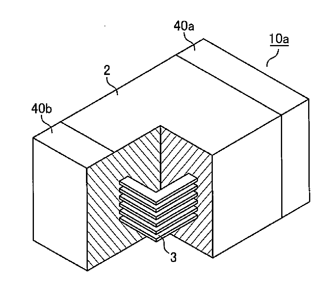
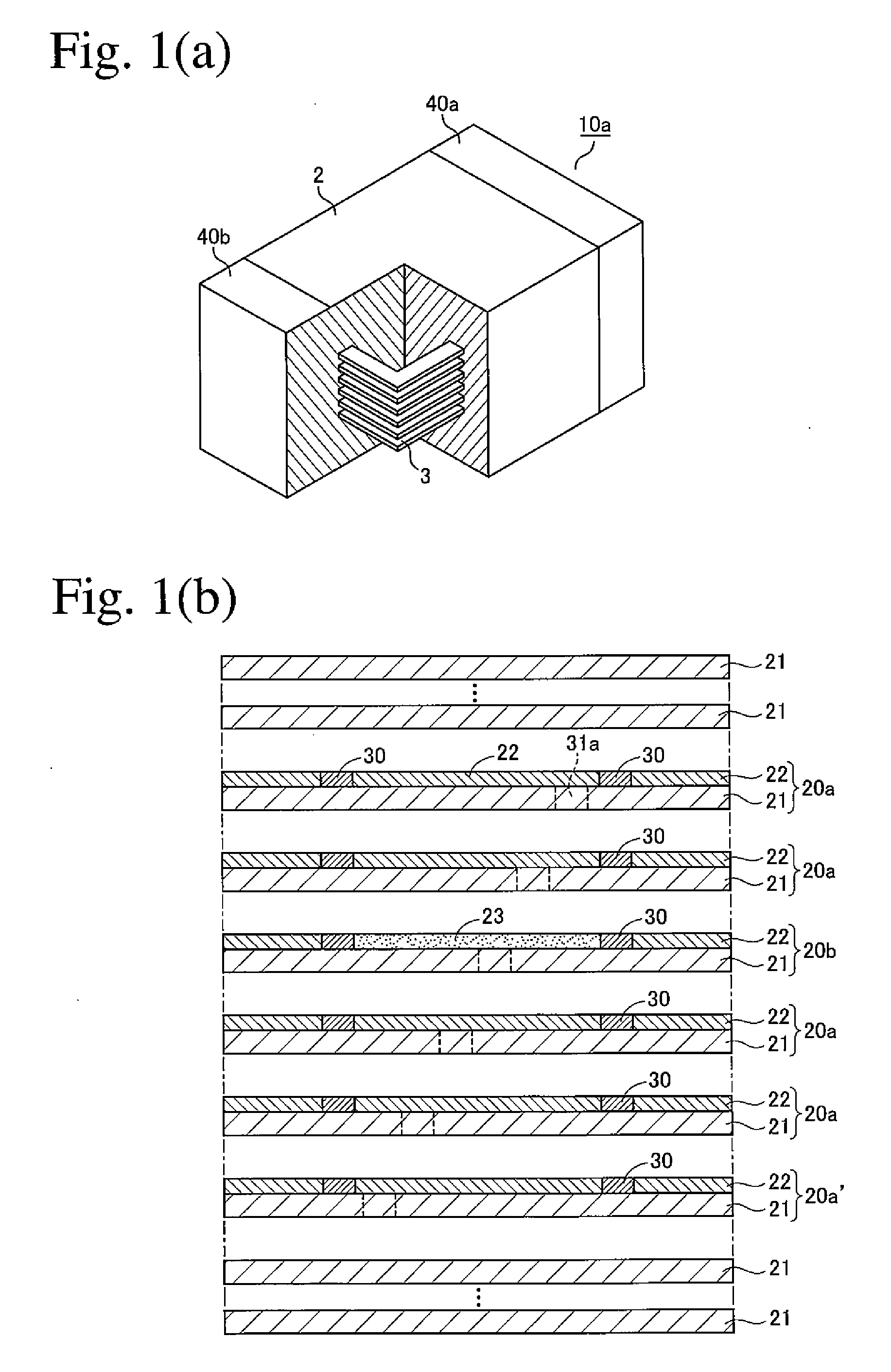
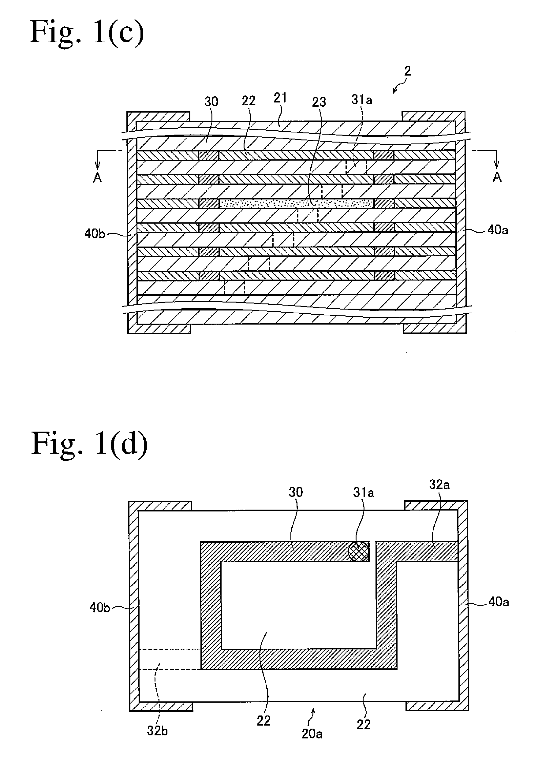
[0102]The laminated inductor 10a shown in FIGS. 1(a)-1(d) was produced by the following procedures. Each ferrite powder of Samples 1 and 6 was pulverized together with a polyvinyl-butyral-based binder and ethanol by a ball mill, and with viscosity adjusted, the resultant slurry was coated on a polyester film by a doctor blade method to form green sheets 21 each having a dry thickness of 30 μm. Each of five green sheets 21 was printed with an Ag paste to form pluralities of substantially one-turn, coil-shaped conductor patterns 30 as thick as 30 μm, thereby forming a sheet having first coil-shaped conductor patterns. A green sheet 21 was printed with an Ag paste to form pluralities of substantially 0.5-turns, coil-shaped conductor patterns 30 as thick as 30 μm, thereby forming a sheet having second coil-shaped conductor patterns.

[0103]The coil-shaped conductor patterns 30l should be as thick as 20 μm or more to reduce DC resistance, but such large thickness provides large difference ...

example 3

[0107]Using the ferrite powder of Sample 6, a laminated inductor was produced in the same manner as in Example 2 except that Zn ferrite having a composition of 48.5% by mol of Fe2O3, 42.7% by mol of ZnO and 8.8% by mol of CuO and a Curie temperature Tc of −60° C. or lower was used for the non-magnetic ceramic paste. The laminated inductor was placed in a constant-temperature chamber to continuously measure inductance at a temperature from −40° C. to +140° C., at a frequency of 1 MHz and current of 1 mA. The change ratio LR of inductance was calculated by the following formula:

LR=(LTn−LT20) / LT20×100(%),[0108]LTn: Inductance at n ° C., and[0109]LT20: Inductance at 20° C.

[0110]FIG. 15 shows the temperature characteristics of the change ratio LR of inductance. FIG. 15 also shows the temperature characteristics of the laminated inductor obtained in Example 2. It is clear from FIG. 15 that the use of Zn ferrite for a magnetic gap reduces inductance change due to the temperature change. EP...


PUM

PropertyMeasurementUnit
magnetic flux densityaaaaaaaaaa
frequencyaaaaaaaaaa
core lossaaaaaaaaaa

Abstract

A low-loss ferrite comprising as main components 46.5-49.5% by mol of Fe2O3, 17-26% by mol of ZnO, 4-12% by mol of CuO, and 0.2% or more and less than 1.2% by mol of CoO, the balance being NiO, and 0.03-1.4% by mass (as SnO2) of Sn based on 100% by mass of the main components, and having an average crystal grain size of 0.7-2.5 μum, and an electronic device obtained by integrally sintering pluralities of layers of this low-loss ferrite and coil-shaped electrodes formed in the laminate.

Description

FIELD OF THE INVENTION[0001]The present invention relates to low-temperature-sinterable ferrite having low loss in a high frequency band with little variation of characteristics under stress, and an electronic device formed as an inductor by such ferrite.BACKGROUND OF THE INVENTION[0002]Various mobile electronic gears (cell phones, mobile information terminals PDA, note-type personal computers, DVD players, CD players, MD players, digital cameras, digital video cameras, etc.) comprise pluralities of DC / DC converters as power conversion apparatuses for converting the voltage of contained cells to operation voltage. In note-type personal computers, for instance, DC / DC converters are arranged near digital signal processors (DSP), micro processing units (MPU), etc.[0003]As one example of DC / DC converters, FIG. 16 shows a step-down DC-DC converter comprising as discrete circuits an input capacitor Cin, an output capacitor Cout, an output inductor Lout, and a semiconductor-integrated circ...

Claims


Application Information

Patent Timeline
Patent Type & Authority Applications(United States)
IPC IPC(8): H01F17/04H01F1/34
CPCC04B35/265H01F2017/0066C04B2235/3239C04B2235/3263C04B2235/3275C04B2235/3279C04B2235/3281C04B2235/3284C04B2235/3293C04B2235/3298C04B2235/5409C04B2235/72C04B2235/724C04B2235/726C04B2235/727C04B2235/785C04B2235/786H01F1/344H01F17/0013H01F17/04C04B2235/3208C04B35/26H01F1/34
Inventor TANAKA, SATORUTACHIBANA, TAKESHI
Owner HITACHI METALS LTD
Why Eureka
Try Eureka