Cleaning of semiconductor processing systems

a technology for processing systems and semiconductors, applied in vacuum evaporation coatings, cleaning of hollow articles, coatings, etc., can solve problems such as electrical short circuits, system filaments that can require replacement, and ion source deposition and contamination

Active Publication Date: 2010-06-24
ENTEGRIS INC
View PDF81 Cites 91 Cited by
  • Summary
  • Abstract
  • Description
  • Claims
  • Application Information

AI Technical Summary

Benefits of technology

[0058]In another aspect, the invention relates to a method of increasing stability of an ion source used to generate plasma, e.g. BF3, AsH3, PH3, GeF4, SiF4, or H2Se, said method comprising cleaning said ion source with a gaseous halide plasma, e.g., XeF2 plasma.

Problems solved by technology

Additionally, the filament of the system can require replacement after operation.
In the ideal case, all feedstock molecules would be ionized and extracted, but in reality a certain amount of feedstock decomposition occurs, which results in the deposition on and contamination of the ion source region.
The residue can form on low voltage insulators in the ion source, causing electrical short circuits, which can interrupt the arc required to produce thermionic electrons.
This phenomenon is generally known as “source glitching,” and it is a major contributor to ion beam instability, and may eventually cause premature failure of the source.
The residue also forms on the high voltage components of the ion implanter, such as the source insulator or the surfaces of the extraction electrodes, causing energetic high voltage sparking.
Such sparks are another contributor to beam instability, and the energy released by these sparks can damage sensitive electronic components, leading to increased equipment failures and poor MTBF.
In addition to the operational difficulties caused by residues in the ion implanter, there are also significant personnel safety issues due to the emission of toxic or corrosive vapors when components are removed for cleaning.
To minimize down time, contaminated ion sources are often removed from the implanter at temperatures significantly above room temperature, which increases the emission of vapors and exacerbates the safety issue.
As a result, these thin film deposits must be removed periodically because they tend to affect the reproducibility of thin film deposition processes by changing the dimensions of the chamber.
Also, the thin film deposits can flake off and contaminate the wafer being processed in the chamber.
Inherent problems associated with this approach include the high volumes of hazardous chemicals that must be used in the cleaning process.
Additionally, the manual breakdown of the processing system and subsequent reassembly is labor-intensive, time-consuming, increases wear on the processing chamber components, and may leave residual contamination within the chamber.
However, a significant amount of hazardous material is moved through the system.
Clearly, the high volume of material utilized in this method not only increases the cost of production but presents ancillary costs relating to the disposal of hazardous materials.
A similar problem exists in the process disclosed in U.S. Pat. No. 5,565,038 wherein a continuous flow of an interhalogen gas is introduced into a processing chamber to be used as a cleaning agent.
Still further, as in the prior art cited above, this method is inherently problematic because of the large quantities of hazardous materials that are utilized, and the associated costs to the manufacturer and / or the environment.
Additionally, the continuous flow cleaning process is performed under very low pressure and cleaning efficiency is reduced under such condition.
However, very high temperatures are required to crack NF3, to release the reactive fluorine ions.
If these temperatures are not reached and / or maintained, hazardous NF3 is exhausted to the surrounding environment.
In addition, the poor reaction selectivity of fluorine ions results in unwanted etching of the quartz reactor.
Still further, depending on the shape of the processing chamber, uniform cleaning is not always predictable or accomplished.
The use of fluorine radicals or fluorine-containing interhalogens for cleaning of semiconductor processing equipment, however, faces practical problems of implementation and commercial viability.
For example, the supply of fluorine radicals or fluorine-containing interhalogens, including ClF3, are highly corrosive, and issues such as compatibility of storage and dispensing vessels, and associated process piping and componentry, require substantial attention and costly solutions.
Further, interhalogen compounds are extremely irritating to human respiratory tracts.
Inadvertent leakage of such highly toxic fluid is therefore highly hazardous to human health.
Further, most interhalogen compounds are liquids at room temperature and are transported in the liquid phase, and the inherent high density of liquids over gases accentuates many of the risks associated with transporting such compounds.

Method used


Image

  • Cleaning of semiconductor processing systems
  • Cleaning of semiconductor processing systems
  • Cleaning of semiconductor processing systems

Examples


example 1

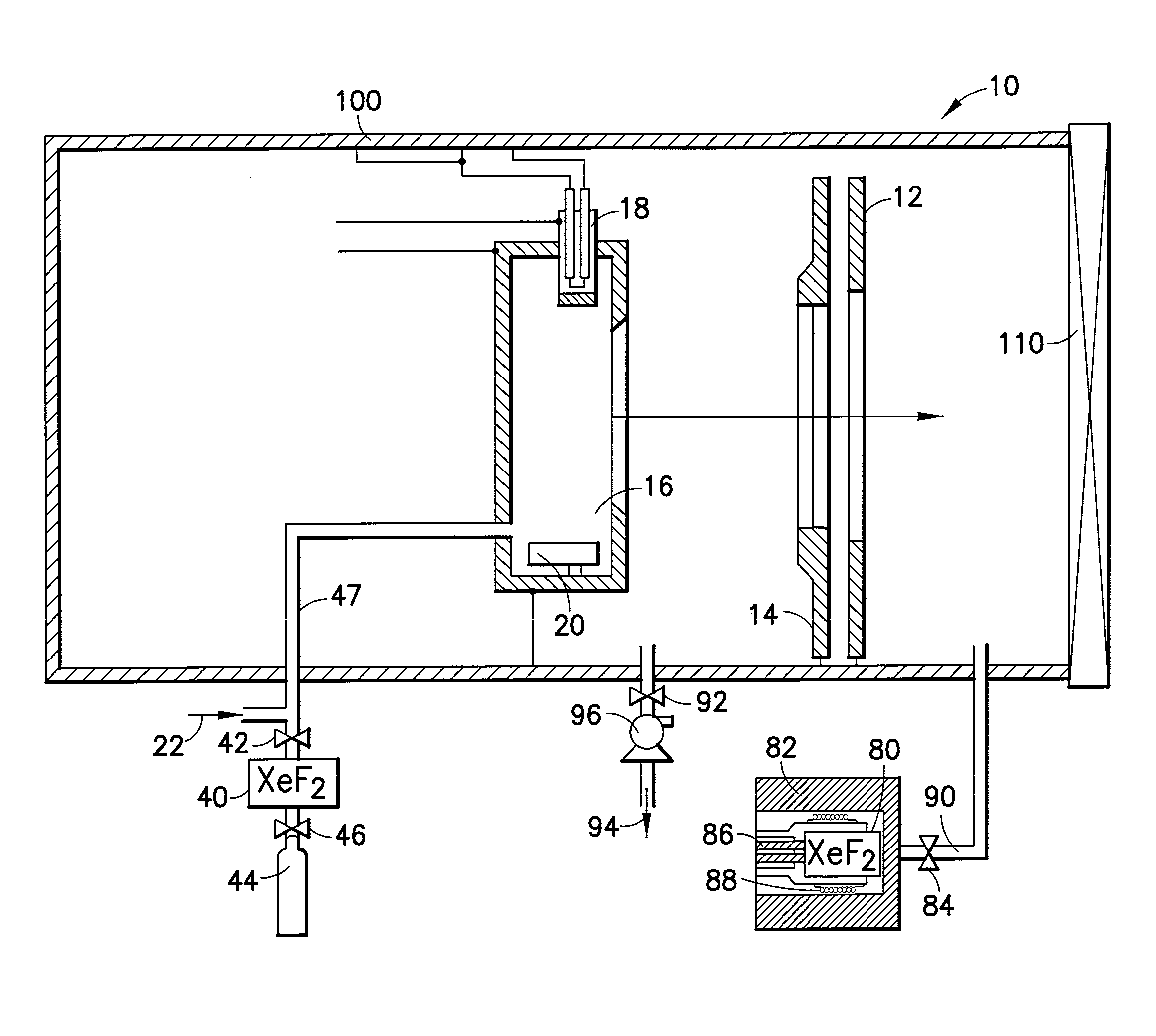
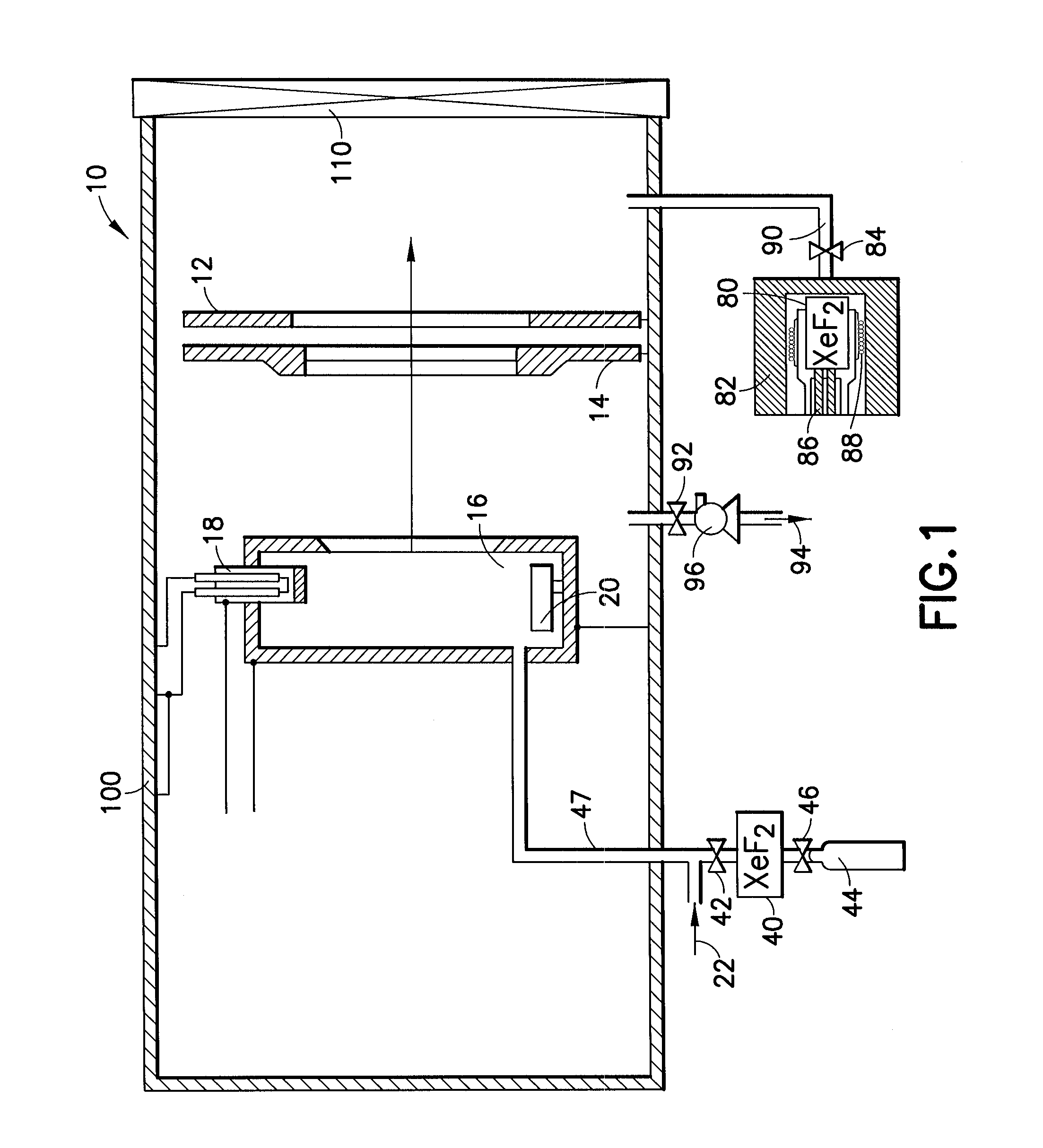
[0237]Test samples were prepared using electron beam deposition of aluminum, boron, tungsten and silicon on glass microscope slides. The aluminum was used as a bottom layer barrier on the glass slide. Some samples were capped with a protective silicon layer while others were left uncapped and allowed to oxidize. The test samples were sequentially placed into an ex situ XeF2 reactor, of a type as shown and described with reference to FIG. 4 hereof, and etched for 16 one-minute pulse-etch cycles at a pressure of 300-400 mTorr at room temperature.

[0238]FIG. 5 is an RGA trace as a function of time showing the efficacy of XeF2 in removing boron residue from an aluminum base layer. The pulse-etch cycles are shown by peaks in the RGA pressure plot in FIG. 5.

[0239]The RGA determined the removal of boron from a glass slide having a base layer of 500 nm of aluminum with 500 nm of boron deposited thereon. There was no silicon capping layer, and therefore the boron could have potentially formed...

example 2

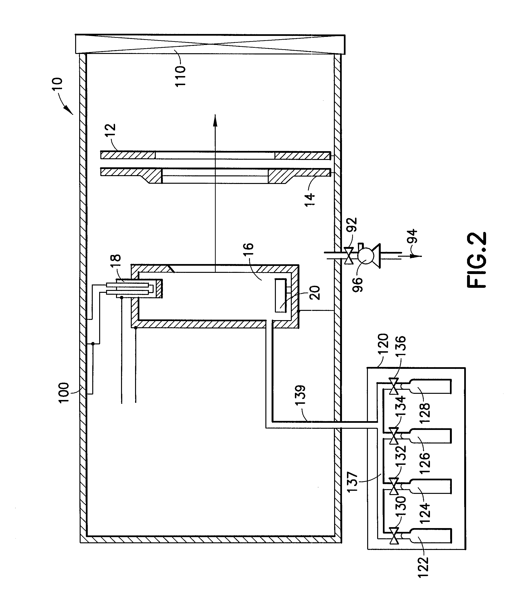
[0242]FIGS. 7 and 8 show data taken on an ion source test apparatus including a single filament Bernas Source with molybdenum arc chamber, and an 80° analyzing magnet with faraday cup measurement of the analyzed beam. A cylinder of XeF2 operating at ambient temperature was installed in the gas box and connected to the ion source with a conventional high conductance gas line.

[0243]FIG. 7 is a graph of beam current, in mA, as a function of time, showing the use of XeF2 plasma to improve stability of the ion source. The source was run with BF3 plasma for about 12 hours at its beam current specification limit, which corresponds to an analyzed beam of about 10 mA of 11B+. When the beam current measurements shown in FIG. 7 began, the source exhibited severe instability at 50 kV extraction voltage, and this instability was not significantly improved by reducing the voltage to 40 kV. After running XeF2 plasma for 20 minutes, the source ran unexpectedly much more stably for about two more ho...

example 3

[0246]While the above Example 1 shows non-reactivity of XeF2 with tungsten on aluminum on a glass slide, it has been found that for an operational ion implantation system, XeF2 is an effective cleaning agent of tungsten deposits generated by reaction of the system components (specifically the arc chamber) with the fluorinated feedstock gas.

[0247]A Bernas source was operated with BF3 feedstock at maximum B+ beam current for 52 hours. The source was removed and two alumina repeller insulators, coated with deposits were removed. Both insulators were weighed prior to cleaning. Insulator 1 (bushing) weighed 6.1676 g prior to cleaning and Insulator 2 (spacer) weighed 7.0662 prior to cleaning. The two insulators were placed in an ex situ vacuum chamber and were cleaned using eleven fill / vent cycles with XeF2, at pressures up to about 3 torr. Each cycle lasted approximately 10 minutes. The mass of XeF2 used in each cycle was about 0.10 g.

[0248]While the cleaning cycles were performed, the R...


PUM

PropertyMeasurementUnit
threshold levelaaaaaaaaaa
temperatureaaaaaaaaaa

Abstract

A method and apparatus for cleaning residue from components of semiconductor processing systems used in the fabrication of microelectronic devices. To effectively remove residue, the components are contacted with a gas-phase reactive material for sufficient time and under sufficient conditions to at least partially remove the residue. When the residue and the material from which the components are constructed are different, the gas-phase reactive material is selectively reactive with the residue and minimally reactive with the materials from which the components of the ion implanter are constructed. When the residue and the material from which the components are constructed is the same, then the gas-phase reactive material may be reactive with both the residue and the component part. Particularly preferred gas-phase reactive materials utilized comprise gaseous compounds such as XeF2, XeF4, XeF6, NF3, IF5, IF7, SF6, C2F6, F2, CF4, KrF2, Cl2, HCl, ClF3, ClO2, N2F4, N2F2, N3F, NFH2, NH2F, HOBr, Br2, C3F8, C4F8, C5F8, CHF3, CH2F2, CH3F, COF2, HF, C2HF5, C2H2F4, C2H3F3, C2H4F2, C2H5F, C3F6, and organochlorides such as COCl2, CCl4, CHCl3, CH2Cl2 and CH3Cl.

Description

STATEMENT OF RELATED APPLICATIONS[0001]This application claims benefit of the following four (4) U.S. Provisional Patent Applications: No. 60 / 795,216 filed on Apr. 26, 2006; No. 60 / 832,037 filed on Jul. 20, 2006; No. 60 / 826,409 filed on Sep. 21, 2006; and No. 60 / 888,311 filed on Feb. 5, 2007.FIELD OF THE INVENTION[0002]The present invention relates to cleaning of semiconductor processing systems.[0003]In various specific aspects, the invention relates to methods and apparatus for cleaning one or more components of an ion implantation system used in the fabrication of a microelectronic device. In additional aspects, the invention relates to methods and apparatus for cleaning one or more components utilized in a CVD system used in the fabrication of a microelectronic device.[0004]In one aspect, the present invention relates to the in situ removal of residue from the system and components contained therein by contacting the system and / or components with a gas-phase reactive material fo...

Claims


Application Information

Patent Timeline
Patent Type & Authority Applications(United States)
IPC IPC(8): B08B5/00
CPCC23C14/564H01J37/32412H01J37/32862C23C16/4405H01L21/302
Inventor DIMEO, FRANKDIETZ, JAMESOLANDER, KARL W.KAIM, ROBERTBISHOP, STEVENNEUNER, JEFFREY W.ARNO, JOSEMARGANSKI, PAUL J.SWEENEY, JOSEPH D.ELDRIDGE, DAVIDYEDAVE, SHARADBYL, OLEGSTAUF, GREGORY T.
Owner ENTEGRIS INC
Why Eureka
Try Eureka