Method, system, and computer program prodcut for lithography simulation in electronic design automation

a technology of electronic design automation and simulation, applied in the field of electronic design automation technology, can solve the problems of parasitic resistance and parasitic capacitance, the cost of manufacturing photomasks, and the inability to meet the requirements of the design process, so as to optimize the performance of the integrated circuit, reduce power consumption, and minimize the amount of parasitic resistance

Active Publication Date: 2010-07-01
CADENCE DESIGN SYST INC
View PDF5 Cites 21 Cited by
  • Summary
  • Abstract
  • Description
  • Claims
  • Application Information

AI Technical Summary

Benefits of technology

[0008]To test an integrated circuit layout, the integrated circuit designer ‘extracts’ parasitic resistance and parasitic capacitance from the integrated circuit layout using an extraction application program. Then, the integrated circuit designer analyzes and possibly simulates the integrated circuit using the extracted parasitic resistance and parasitic capacitance information. If the parasitic resistance or parasitic capacitance causes undesired operation of the integrated circuit, then the layout of the integrated circuit must be changed to correct the undesired operation. Furthermore, minimizing the amount of parasitic resistance and parasitic capacitance can optimize the performance of the integrated circuit by reducing power consumption or increasing the operating speed of the integrated circuit.
[0017]Therefore, it is desirable to devise a method, system, and computer program product to better simulate the photolithography process with better accuracy and efficiency. More particularly, some embodiments achieve better accuracy by accommodating some or all relevant effects without having to solve the physics-based partial differential equations. Some embodiments maintains better efficiency by starting with a physics-based governing equation incorporating relevant effects while employing model reduction techniques to improve the efficiency.

Problems solved by technology

However, the geometry of a real conductor, its material composition, and its interaction with other nearby circuit elements will create some parasitic resistance and parasitic capacitance.
The parasitic resistance and parasitic capacitance affect the operation of the designed integrated circuit.
Lithography simulation has recently gathered more attention in the past decades or two because of the increasing cost in manufacturing photomasks and development time to redesign and remanufacture a revised set of photomasks in case of a error in the design of the masks.
Nonetheless, RET may pose further challenges to the integrated circuit (IC) design due to the continual pursuit for smaller geometry size and the use of shorter wavelength on the lithographic tools such as the 193 nm λ ultra-high numerical aperture (NA) lithography or even the Extreme Ultra Violet lithography, especially in the deep submicron and increasing clock frequency designs.
However, larger numerical aperture also decreases the depth of focus, and such decreased depth of focus causes the lithographic tools' ability to print accurate circuits to be more sensitive to the topographical variation of the films on the wafer.
Experience indicates that even the state-of-the-art solvers are too slow or memory-bounded to handle a medium-size mask structure.
Nonetheless, this is clearly not the case for phase-shifted masks.
Moreover, these assumptions may no longer be true even for the binary mask for 45 nm or smaller technology nodes.
It has been demonstrated that the Kirchhoff approximation, or the thin mask model, fails when the thickness of the mask is greater than the wavelength of the incidence wave of the lithographic equipment.
It has also been demonstrated that the Kirchhoff approximation or the thin mask model fails to provide satisfactory solution when the size of the aperture is smaller than the wavelength of the incidence wave of the lithographic equipment.
The first approach generally uses the boundary layer method which requires a 3D solver as the core engine and is thus CPU (central processing unit) intensive.
Nonetheless, most, if not all, of the approaches suffer from some major drawbacks.
Mathematically and practically, this is a multi-dimensional curve fitting process for some intrinsic parameters which include, for example, width and height of the rectangular aperture or opening, the constant transmission coefficient, the profile of the phase-shift mask, and a host of illumination parameters (e.g., on-axis or off-axis, shape and size of the source, etc.) The accuracy of such a curve-fitting process has been demonstrated to be unreliable.
Moreover, in order to make this multi-dimensional curve fitting process tractable, most, if not all, of these modified thin-mask approaches considers only one aperture or opening at a time and do not account for coupling among various openings and features in the mask.
In addition, these multi- or high-dimensional piecewise constant curve fitting functions may be relatively simpler and efficient, but they may not be sufficiently accurate to meet the design requirements.
For example, it is hard to account for effects such as diffraction, coupling, or polarization with these modified thin-mask models.
One could use more sophisticated curve fitting techniques to improve the accuracy, but the high-dimensional curve fitting is typically not sufficiently robust or efficient.
Hence these modified thin-mask models are typically limited only to small number of parameters in small mask structures.
That is, these modified thin-mask models are essentially a result of a multi-dimensional curve fitting process which is known to be numerically unreliable and CPU intensive.
It is also very difficult to assert the accuracy of such modified thin-mask models, and hence the fidelity of the models is not guaranteed.
As a consequence, many important effects, such as couplings among openings and features and polarization, are not well modeled in the modified thin-masks model.
For more advanced technology nodes, when the feature size is 45 nm or below, the poor accuracy of such modified thin-mask or modified Kirchhoff models would render these models much less useful than they are at 65 nm or above technology nodes.
Nonetheless, starting from 45 nm technology nodes, the mask feature sizes become increasingly smaller than the wave length(s) of the lithographic equipment, and this continual shrinkage of the feature sizes has rendered the accuracy of the Kirchhoff mask models even more questionable.

Method used


Image

  • Method, system, and computer program prodcut for lithography simulation in electronic design automation
  • Method, system, and computer program prodcut for lithography simulation in electronic design automation
  • Method, system, and computer program prodcut for lithography simulation in electronic design automation

Examples


Embodiment Construction

[0032]The invention is described with reference to specific embodiments. It will, however, be evident that various modifications and changes may be made thereto without departing from the broader spirit and scope of the invention. The reader is to understand that the specific ordering and combination of process actions shown in the process flow diagrams and system components in component diagrams described herein are merely illustrative, and the invention can be performed using different, additional, or different combinations / ordering of process actions and components. The specification and drawings are, accordingly, to be regarded in an illustrative rather than restrictive sense.

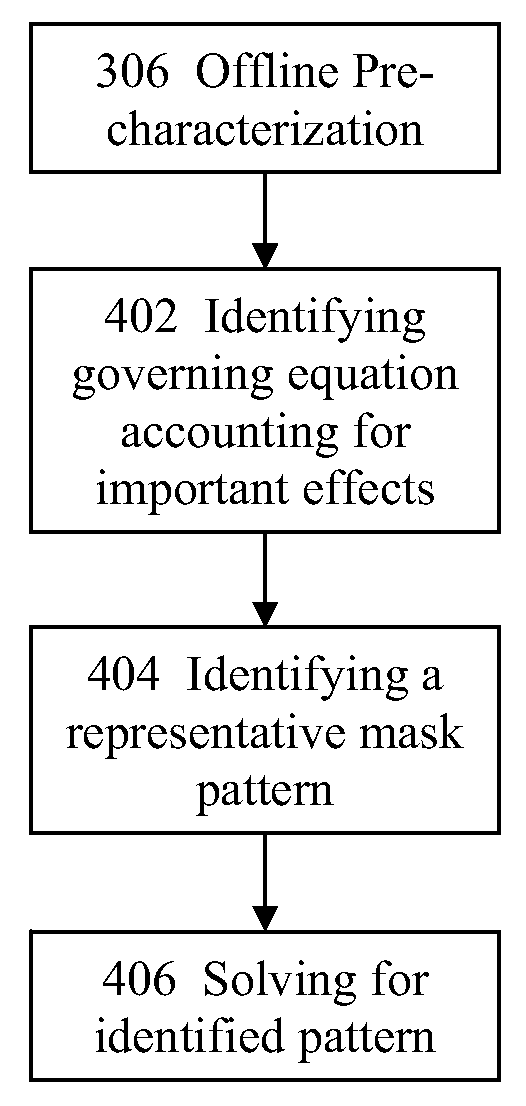
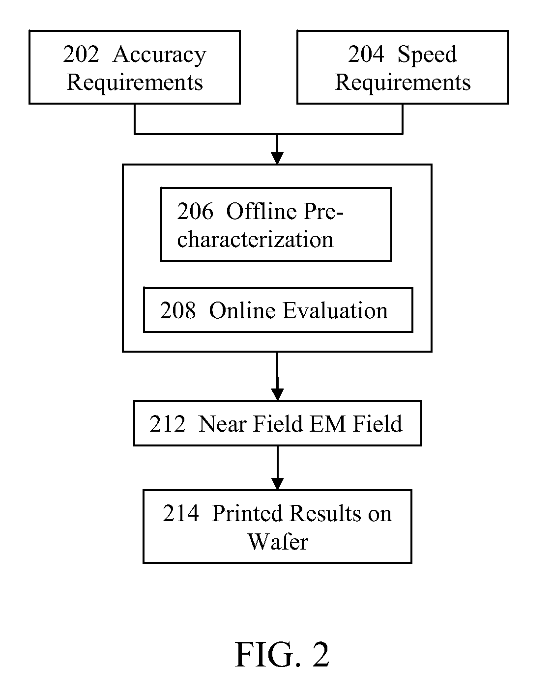
[0033]Various embodiments of the invention which are directed to an improved method, system, and computer program product for implementing a process for lithographic simulation. The process comprises an act of offline pre-characterization which comprises generating a library or a library of model(s) for one...


PUM


Abstract

Disclosed are improved methods, systems, and computer program products for lithographic simulation of an electronic circuit design. Various embodiments of the present invention identifies a mask pattern, performs offline precharacterization for the mask pattern by solving an equation which models a solution for the mask pattern and an interaction between the mask pattern and one or more effects, performs online evaluation based at least upon a parameterized form of the equation, determines a field around the mask pattern based at least upon the act of performing the online evaluation, and stores a result of the act of determining an electromagnetic field around the mask pattern in a tangible computer readable or usable medium

Description

CROSS-REFERENCE TO RELATED APPLICATION(S)[0001]Certain aspects in some embodiments of this Application are related to and disclosed in U.S. application Ser. Nos. 10 / 932,406 which is entitled “CIRCUIT ANALYSIS UTILIZING RANK REVEALING FACTORIZATION” and was filed on Sep. 2, 2004, the content of which is incorporated by reference in their entirety in this Application.BACKGROUND AND SUMMARY[0002]The invention relates to technology for designing and verifying an integrated circuit (“IC”) design.[0003]An IC has a large number of electronic components, such as transistors, logic gates, diodes, wires, etc., that are fabricated by forming layers of different materials and of different geometric shapes on various regions of a silicon wafer. The design of an integrated circuit transforms a circuit description into a geometric description called a layout. The process of converting specifications of an integrated circuit into a layout is called the physical design. After the layout is complete,...

Claims


Application Information

Patent Timeline
Patent Type & Authority Applications(United States)
IPC IPC(8): G06F17/10G06F17/50
CPCG03F7/705
Inventor ZHU, ZHENHAI
Owner CADENCE DESIGN SYST INC
Why Eureka
Try Eureka