Organic electroluminescent device

a technology of electroluminescent devices and organic materials, applied in the direction of electroluminescent light sources, organic semiconductor devices, thermoelectric devices, etc., to achieve the effect of improving driving durability and lowering driving voltag

Inactive Publication Date: 2010-08-05
UDC IRELAND
View PDF9 Cites 5 Cited by
  • Summary
  • Abstract
  • Description
  • Claims
  • Application Information

AI Technical Summary

Benefits of technology

[0131]It is preferable that the thicknesses of the hole injection layer and the hole transport layer are respectively 500 nm or less, from the viewpoint of lowering the driving voltage.
[0132]The thickness of the hole transport layer is preferably 1 nm to 500 nm, more preferably 5 nm to 200 nm, and even more preferably 5 nm to 100 nm. The thickness of the hole injection layer is preferably 0.1 nm to 500 nm, more preferably 0.5 nm to 400 nm, and even more preferably 1 nm to 300 nm.
[0133]Each of the hole injection layer and hole transport layer may have a single layer structure formed from one or two or more species of the materials mentioned above, or may also have a multilayer structure including plural layers having identical composition or different compositions.
[0134]Electron Injection Layer and Electron Transport Layer
[0135]The electron injection layer and the electron transport layer are layers having a function of receiving electrons from the cathode 18 or from the cathode side, and transporting the electrons to the light emitting layer side (anode side). The electron injection layer and the electron transport layer are preferably layers containing, specifically, a triazole derivative, an oxazole derivative, an oxadiazole derivative, an imidazole derivative, a fluorenone derivative, an anthraquinodimethane derivative, an anthrone derivative, a diphenylquinone derivative, a thiopyrane dioxide derivative, a carbodiimide derivative, a fluorenylidenemethane derivative, a distyrylpyrazine derivative, an aromatic ring tetracarboxylic acid anhydride of naphthalene, perylene or the like, a phthalocyanine derivative, or various metal complexes represented by metal complexes of 8-quinole derivatives, metal phthalocyanine, and metal complexes having benzoxazole or benzothiazole as the ligand, an organic silane derivative, or the like.
[0136]The electron injection layer and / or electron transport layer of the organic EL device of the invention preferably contains an electron donating dopant from the viewpoint of lowering the voltage and improving the driving durability.

Problems solved by technology

However, in practice, an organic EL device achieving improvements in the luminescence efficiency and durability, by allowing the entire light emitting layer to emit light by precisely controlling the carrier balance in the light emitting layer, is not found.

Method used


Image

  • Organic electroluminescent device
  • Organic electroluminescent device
  • Organic electroluminescent device

Examples


example 1

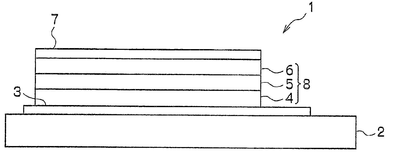
[0165]An ITO film (thickness 100 nm) is formed as an anode on a supporting substrate (material: glass), and then using a vacuum deposition apparatus (1×10⁻⁶ torr), co-deposition was performed thereon using 2-TNATA (4,4′,4″-tris(2-naphtylphenylamino)triphenylamine), and F4-TCNQ (tetrafluorotetracyanoquinodimethane) in an amount of 1.0% by mass based on 2-TNATA, to form a hole injection layer having a thickness of 160 nm. Subsequently, a film of NPD (N,N′-dinaphthyl-N,N′-diphenyl-[1,1′-biphenyl]-4,4′-diamine) was formed as a hole transport layer having a thickness of 10 nm. The structural formulas of 2-TNATA, F4-TCNQ and NPD are as follows.

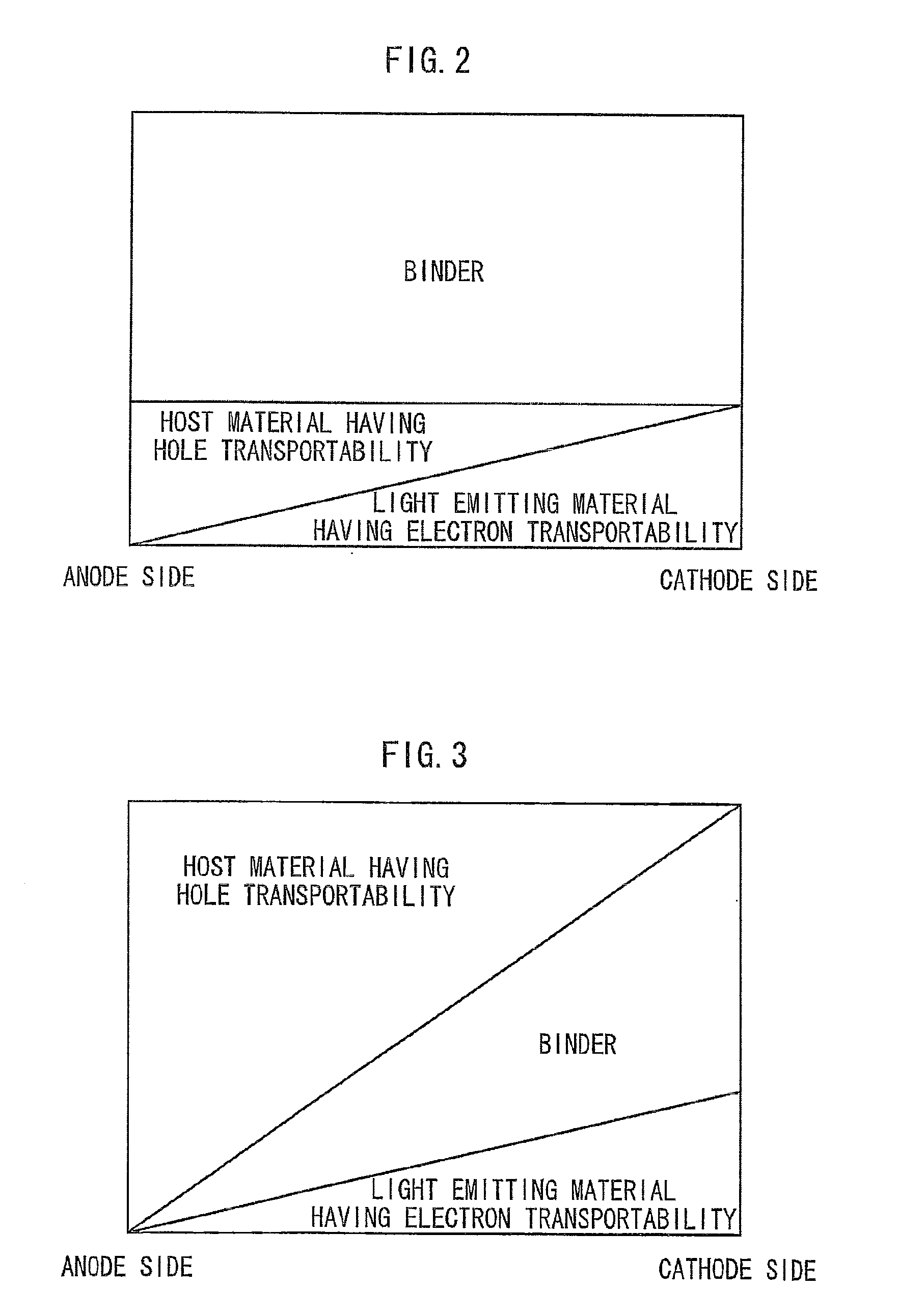
[0166]After forming the hole transport layer, a light emitting layer was laminated thereon. The light emitting layer was formed as a mixed layer (thickness 60 nm) by co-deposition using mCP (N,N′-dicarbazolyl-3,5-benzene) as a host material having hole transportability, Pt-1 as a light emitting material (blue light emitting material) having electron...

example 2

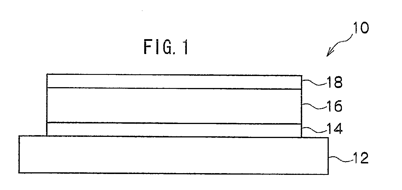
[0177]A blue emitting organic EL device having the same layer configuration as in Example 1 was produced in the same manner as in Example 1, except that silicon oxide (inorganic binder) was used instead of the compound A (organic binder) used in the case of forming the light emitting layer in Example 1. The respective concentration distributions of the materials in the light emitting layer are presented in FIG. 4B. The layer configuration, thickness of each of the layers, and the like of the luminescent device are as follows.

ITO (100 nm) / 2-TNATA+1.0% F4-TCNQ (160 nm) / NPD (10 nm) / 26%→0% mCP+74% inorganic binder+0%→26% Pt-1 (60 nm) / BAlq (40 nm) / LiF (1 nm) / Al (100 nm)

[0178]The external quantum efficiency and the luminance half-life of the obtained organic EL device were measured under the same conditions as in Example 1 (hereinafter, the same), and as a result, the external quantum efficiency at 360 cd / m2 was 12.5%, while the luminance half-life was 1800 hours.

example 3

[0179]An organic EL device having the same layer configuration and thicknesses as in the organic EL device of Example 1, except for the light emitting layer, was produced. The light emitting layer was formed using the same materials as those used in Example 1, such that the respective materials have concentration distributions as shown in FIG. 4C. The layer configuration, thickness of each of the layers, and the like of the luminescent device are as follows.

ITO (100 nm) / 2-TNATA+1.0% F4-TCNQ (160 nm) / NPD (10 nm) / 100%→0% mCP+74% organic binder+0%→26% Pt-1 (60 nm) / BAlq (40 nm) / LiF (1 nm) / Al (100 nm)

[0180]The external quantum efficiency and the luminance half-life of the obtained organic EL device were measured, and as a result, the external quantum efficiency at 360 cd / m2 was 13.5%, while the luminance half-life was 2000 hours.

[0181]It is conceived that when the concentration of the binder in the light emitting layer was gradually decreased from the cathode side toward the anode side, ...


PUM


Abstract

An organic electroluminescent device 10 has an anode 14, a cathode 18 disposed facing the anode, and an organic layer 16 that is sandwiched between the anode and the cathode and that includes at least a light emitting layer, wherein the light emitting layer includes a light emitting material having electron transportability, a host material having hole transportability and an electrically inert material, and the concentration of the light emitting material having electron transportability gradually decreases from the cathode side toward the anode side. Preferably, the concentration of the electrically inert material also gradually decreases from the cathode side toward the anode side.

Description

BACKGROUND OF THE INVENTION[0001]1. Field of the Invention[0002]The present invention relates to an organic electroluminescent device.[0003]2. Description of the Related Art[0004]In recent years, light emitting apparatuses utilizing organic electroluminescent devices (organic EL devices) have been developed. FIG. 6 schematically shows the configuration of an organic EL device 1. On a substrate 2 made of glass or the like, an anode 3, organic EL layers 8 (hole transport layer 4, light emitting layer 5 and electron transport layer 6), a cathode 7 and the like are formed in layers. In the drawing, partitions, insulating films, sealing members and the like are not shown. The two electrodes 3 and 7 are connected to external lines through the lead lines (terminals) of the electrodes. When an electric field is applied to the electrodes, holes and electrons recombine in the light emitting layer 5 in the region sandwiched between the electrodes 3 and 7 to emit light.[0005]In the case of prod...

Claims


Application Information

Patent Timeline
Patent Type & Authority Applications(United States)
IPC IPC(8): H01L51/54
CPCH01L51/005H01L51/0071H01L51/0081H01L51/0087H05B33/18H01L51/5012H01L2251/308H01L2251/5346H01L2251/552H01L51/0094H10K85/60H10K85/657H10K85/324H10K85/346H10K85/40H10K50/11H10K2101/80H10K2102/103H10K2101/30
Inventor KINOSHITA, MASARUTOBISE, MANABU
Owner UDC IRELAND
Why Eureka
Try Eureka