Memory element and memory device

a memory element and memory technology, applied in semiconductor devices, digital storage, instruments, etc., can solve the problems of low performance for retaining information, change in resistance value, and inability to retain information, and achieve improved retaining performance in erased states and high resistance states. , the effect of favorable retaining property

Active Publication Date: 2010-08-05
SONY CORP
View PDF4 Cites 65 Cited by
  • Summary
  • Abstract
  • Description
  • Claims
  • Application Information

AI Technical Summary

Benefits of technology

[0013]Here, in a case where an anode electrode (the second electrode) is biased to a lower potential by erasing operation, Al included in the ion source layer does not dissolve in the ion source layer but is oxidized at an interface between the ion source layer which behaves in a solid electrolyte-like manner and the anode, and forms a chemically-stable oxide film. Thereby, a retaining performance in an erased state (the high-resistance state) is improved, and a favorable retaining property is obtained in any resistance value range. Also, a change and deterioration in device characteristics in a case in which writing and erasing cycles are repeated are reduced. Meanwhile, Mg may be added in place of Al.
[0014]According to the memory element or the memory device of the present invention, Al (aluminum) is contained in the ion source layer together with the ion conductive material and the metal element to be ionized. Therefore, the retaining performance of the resistance value in the high-resistance state (the erased state) improves in particular. In addition, since the retaining property of the resistance value improves, an intermediate state between the high-resistance state and the low-resistance state can be generated, by adjusting, for example, an erasing voltage at the time when it is changed from the low-resistance state to the high-resistance state. Therefore, multi-valued memory is possible, and it is possible to realize large-capacity. Moreover, since long-repetition is possible and short-pulse high-speed driving operation is possible, it exhibits an effect that it is superior also in the retaining property of the resistance value in high speed operation.

Problems solved by technology

However, the memory elements having the configurations described above each has a problem that the resistance value changes and information is not retained when it is left for a long period of time or is left in a temperature atmosphere which is higher than room temperature, in a stored state (e.g., “1”) in which the resistance value of the ionic conductor is low in resistance or in an erased state (e.g., “0”) in which it is in high in resistance value.
In a case where performance for retaining information is low as previously described, device characteristics are insufficient to be used in the nonvolatile memory.
Thus, there has been a problem that retaining of the intermediate resistance values between the high-resistance state and the low-resistance state is difficult, and thus realization of the multi-valued memory is difficult.

Method used


Image

  • Memory element and memory device
  • Memory element and memory device
  • Memory element and memory device

Examples


example 1

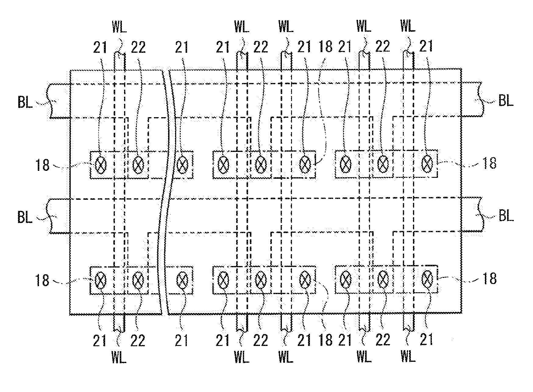
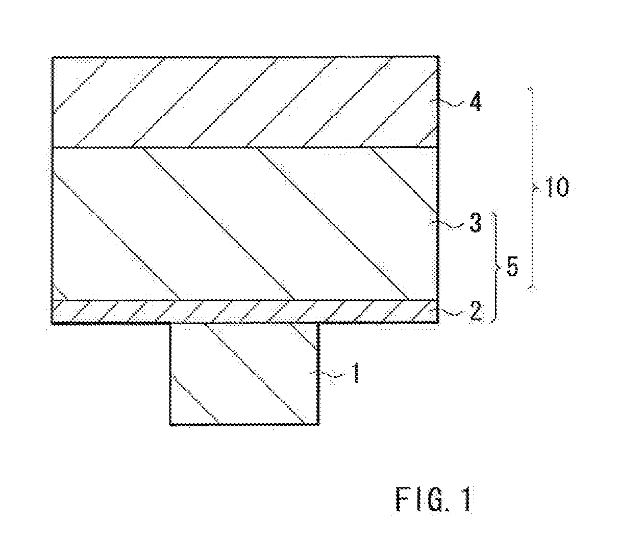
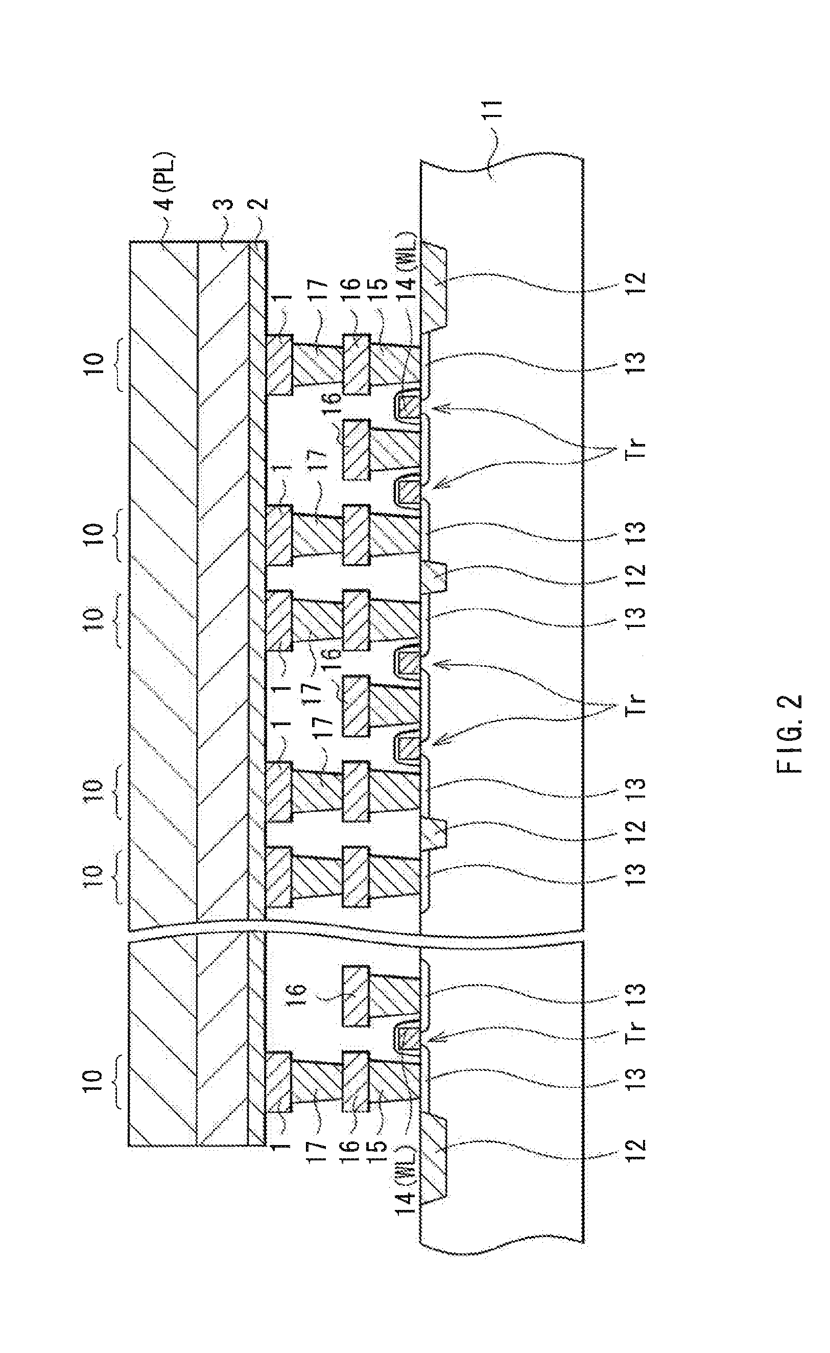
[0067]As illustrated in FIG. 2 and FIG. 3, the MOS transistor was first formed on the semiconductor substrate 11. Then, an insulating layer was formed to cover a surface of the semiconductor substrate 11, and a via-hole was formed on the insulating layer. Subsequently, the inside of the via-hole was filled with an electrode material consisting of W (tungsten) with a CVD (Chemical Vapor Deposition) method, and a surface thereof was planarized with a CMP (Chemical Mechanical Polishing) method. In addition, these processes were repeated to form the plug layer 15, the metal wiring layer 16, the plug layer 17, and the lower electrode 1, and further, the lower electrode 1 was patterned for each memory cell. A size of an opening of the lower electrode 1 was configured with a diameter of 300 nm. Then, etching was performed by about 1 nm with reverse sputtering utilizing a RF power source, in order to remove an oxide on an upper surface of the lower electrode 1. At this time, a surface of th...

examples 2 to 5

[0074]In the Examples 2 to 5, other transition metal elements Ta, Cr, Ti, and W were used as the metal element to be ionized in the ion source layer 3. The film-thickness was 45 nm each.

[0075]Example 2: Ta 20%-Te 40%-Al 40% (atomic %)

[0076]Example 3: Cr 30%-Te 30%-Al 40% (atomic %)

[0077]Example 4: Ti 30%-Te 30%-Al 40% (atomic %)

[0078]Example 5: W 15%-Zr 5%-Nb 5%-Te 35%-Al 40% (atomic %)

examples 10 to 15

[0086]Films having the following composition ratios with the film-thicknesses of 45 nm were formed by using Zr and Cu as the metal element to be ionized of the ion source layer 3, respectively. Ratios of Zr and Cu were each represented by a fraction ratio of Zr / (Cu+Zr), and were varied from 1, 0.69, 0.5, 0.32, and 0.15 to 0.

[0087]Example 10: Zr 16%-Te 44%-Al 40% (atomic %)

[0088]Example 11: Zr 11%-Cu 5%-Te 44%-Al 40% (atomic %)

[0089]Example 12: Zr 8%-Cu 8%-Te 44%-Al 40% (atomic %)

[0090]Example 13: Zr 10%-Cu 21%-Te 29%-Al 44% (atomic %)

[0091]Example 14: Zr 5%-Cu 28%-Te 28%-Al 39% (atomic %)

[0092]Example 15: Cu 45%-Te 23%-Al 32% (atomic %)


PUM


Abstract

The capability of retaining a resistance value of a stored state and an erased state is improved in a resistance variation-type memory device. A memory layer 5 including a high-resistance layer 2 and an ion source layer 3 is provided between a lower electrode 1 and an upper electrode 4. The ion source layer 3 contains Al (aluminum) as an additive element together with an ion conductive material such as S (sulfur), Se (selenium), and Te (tellurium) (chalcogenide element) and a metal element to be ionized such as Zr (zirconium). Since Al is included in the ion source layer 3, the high-resistance layer which includes Al (Al oxide) is formed on an anode in erasing operation. Thus, a retaining property in a high-resistance state improves, and at the same time, an operating speed is improved.

Description

TECHNICAL FIELD[0001]The present invention relates to a memory element and a memory device capable of storing binary or more information by a change in an electrical characteristic of a memory layer including an ion source layer.BACKGROUND ART[0002]DRAM (Dynamic Random Access Memory), which is fast in operation and high in density, has been widely used as RAM (Random Access Memory: random access memory) in information devices such as a computer. However, since a manufacturing process of the DRAM is complex as compared with an ordinary logic circuitry LSI (Large Scale Integration) used in electronic devices or with a signal process, a production cost is high. Also, the DRAM is a volatile memory in which information is lost when power is turned off. Thus, it is necessary to frequently perform refresh operation, that is, to perform operation of reading out the written information (data), performing re-amplification, and performing rewrite again.[0003]Accordingly, a flash memory, FeRAM ...

Claims


Application Information

Patent Timeline
Patent Type & Authority Applications(United States)
IPC IPC(8): G11C11/00H01L45/00
CPCG11C11/5614G11C13/0011H01L27/101H01L27/2436H01L27/2472H01L45/085H01L45/1625H01L45/1266H01L45/141H01L45/142H01L45/143H01L45/144H01L45/145H01L45/1233H10B63/82H10B63/30H10N70/245H10N70/8416H10N70/826H10N70/8833
Inventor OHBA, KAZUHIROMIZUGUCHI, TETSUYAYASUDA, SHUICHIRO
Owner SONY CORP
Why Eureka
Try Eureka