

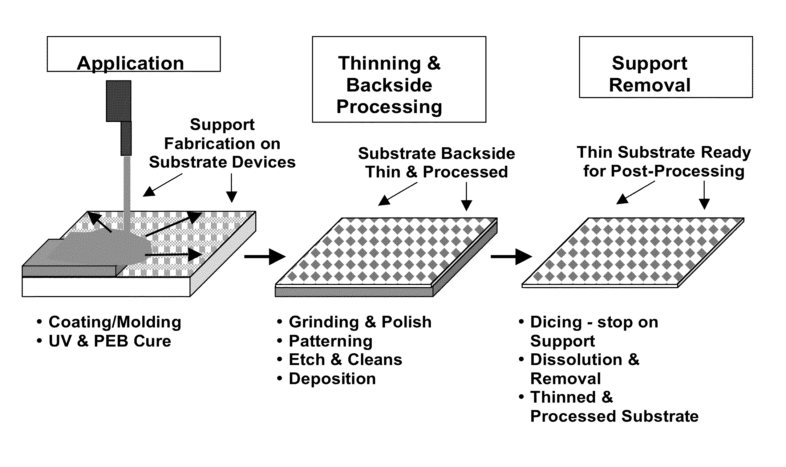
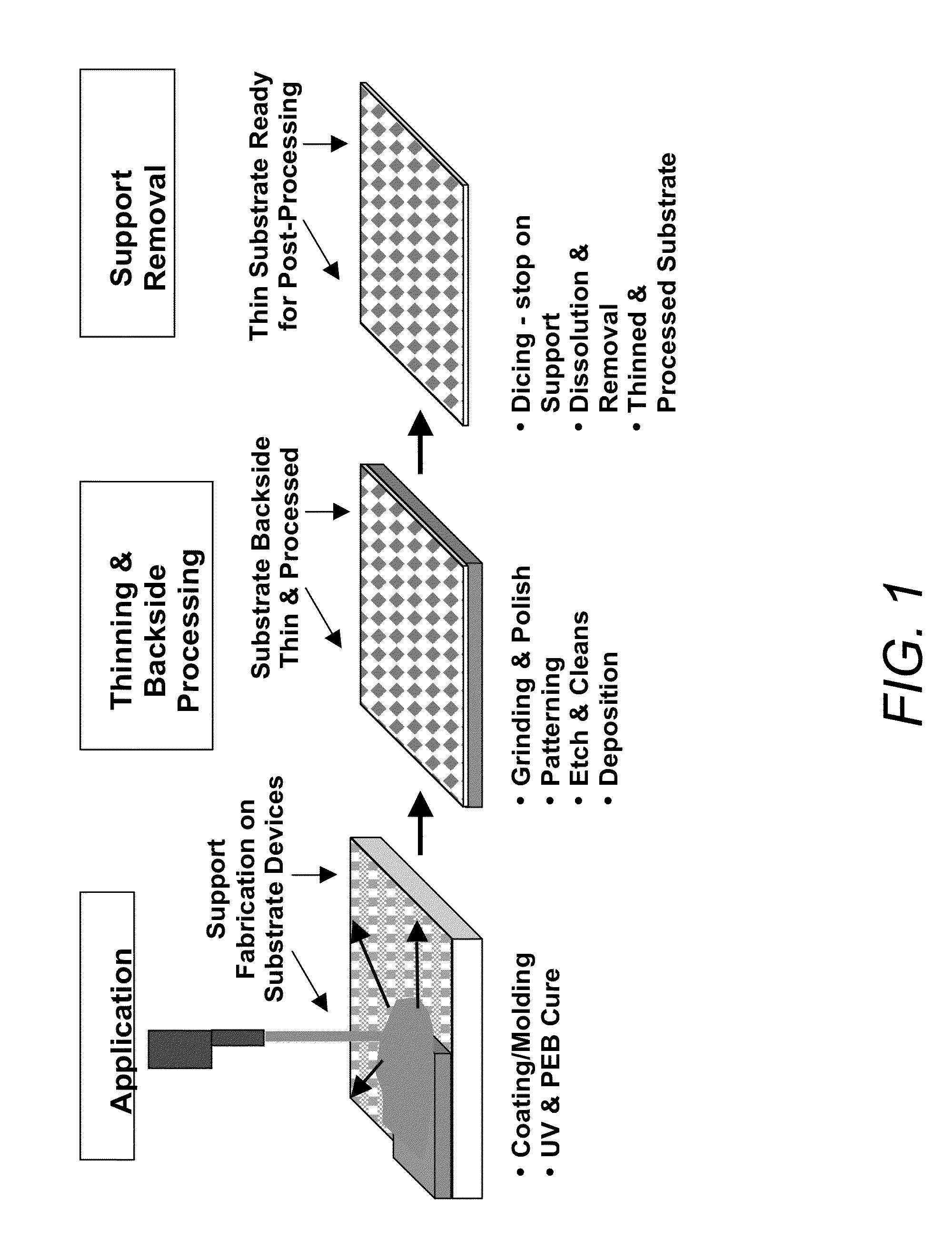
Rapid fabrication of a microelectronic temporary support for inorganic substrates
a technology of microelectronics and substrates, applied in the direction of manufacturing tools, auxillary shaping apparatus, coatings, etc., can solve the problems of limited ability to reduce substrate dimensions to ultra-thin dimensions, limited conventional methods for thinning, and inability to achieve these objectives, etc., to achieve rapid installation, promote high processing throughput, and eliminate process bottlenecks and surface damage
- Summary
- Abstract
- Description
- Claims
- Application Information
AI Technical Summary
Benefits of technology
Problems solved by technology
Method used
Image

Examples
example 1
Compositions with Various Photoinitiators to Achieve Rapid Curing
[0105]In this experiment, the monomer, n-n-dimethylacrylamide (DMAA) is used as a base resin for the initiator to cause the cure reaction. The resin system is mixed and applied to glass substrates of 1 mm thickness. Exposure conditions with the necessary ultraviolet source is conducted for 5 min and followed with a 100 degree centigrade hot plate exposure. Curing observations are recorded for each stage. The initiators are listed in Table 2 and results are indicated in Table 3.
TABLE 2Photoinitiator types and concentrations used with acrylic monomer.Wave-Concen-lengthtrationInitiatorChemistry(nm)(%)IrgacureBAPO / ∝-hydroxyketone (Irgacure3650.5, 2, 52022819:Darocure 1173, 20:80)Irgacure 819Phosphine oxide, phenyl bis (2,4,6-3650.5, 2, 5trimethyl benzoyl)Irgacure2-Hydroxy-1-[4-(2-3650.5, 2, 52959hydroxyethoxy)phenyl]-2-methyl-1-propanoneDarocure2-Hydroxy-2-methyl-1-phenyl-1-3650.5, 2, 51173propanoneIrgacure 250Iodonium, (4...
example 2
Compositions with Various Monomers to Achieve Reduced Internal Stress
[0107]In this experiment, various monomers are used as a base resin for the initiator Irgacure 2022 to cause the cure reaction in a manner which results in a relative reduced level of stress. The resin system is mixed and applied to glass substrates of 100 um thickness. Exposure conditions with a 365 nm ultraviolet source is conducted for 5 min and followed with a 100 degree centigrade hot plate exposure. Stress is observed as a bending of the substrate and is recorded for each mixture. The monomers listed in Table 1 are tested for UV curing, heat curing, and stress observations throughout the experiment.
TABLE 4Monomers and results for UV and thermal cure,stress measurement to 200 C.Iden-tityProduct NameChemistryManufacturerAAgeflex ™n,n-Ciba Specialty ChemicalsNDMAA puredimethylacrylamideCorporation(DMAA, CAS(www.cibasc.com)#2680-03-7)BRocryl ™ 400hydroxyethylRohm & Haas Companymethacrylate(www.rohmhaas.com)(CAS #...
example 3
Compositions with High TAN Rosins to Achieve Moisture Resistance & Alkali Solubility
[0109]In this experiment, various rosins with high TAN values are added to a base acrylic mixture, cured, and tested against the based product to enhance moisture resistance and alkali solubility. The substances are described as item #1 in Table 1. The substances and results are listed in Table 6.
TABLE 6Results for cure, moisture resistance, and TMAH dissolution ofrosin additives.TMAHIdentityMoistureEnhanced(TAN) valueManufacturerUV CureResistantSolubilitySylvaprint ™ArizonaYesYesYes8200 (199)Sylvaprint ™ArizonaNo, requiresYesYes8250 (246)high heat cureResinall ™ResinallNo, requiresYesNoC56-243high heat cure(300)Resinall ™ResinallNo, requiresNoNo833 (200)high heat cure
[0110]Results which enhance moisture resistance and TMAH solubility from Example 3 suggest promoting the additive Sylvaprint™8200 in the acrylic mixture. All other TAN additives either did not provide the cure objective, did not provide...
PUM
| Property | Measurement | Unit |
|---|---|---|
| melting point | aaaaa | aaaaa |
| thicknesses | aaaaa | aaaaa |
| thicknesses | aaaaa | aaaaa |
Abstract
Description
Claims
Application Information