Method for growing zinc-oxide-based semiconductor device and method for manufacturing semiconductor light emitting device

a technology of zinc oxide-based semiconductors and light-emitting devices, which is applied in the direction of semiconductor/solid-state device manufacturing, semiconductor devices, electrical equipment, etc., can solve the problems of low productivity, high equipment cost, and the inability to grow zinc-oxide-based single crystal directly using the mocvd method

Inactive Publication Date: 2010-11-25
STANLEY ELECTRIC CO LTD
View PDF12 Cites 13 Cited by
  • Summary
  • Abstract
  • Description
  • Claims
  • Application Information

AI Technical Summary

Benefits of technology

[0018]a buffer layer grown on the substrate at a growth temperature in the range of 250° C. to 450° C. using a polar oxygen material and a metalorganic compound contai

Problems solved by technology

The MBE method is a crystal growth method in an ultrahigh vacuum, and it has problems that an apparatus is expensive and productivity is low.
However, utilizing the MOCVD method to directly grow a zinc-oxide-based single crystal (which will be also referred to as a ZnO-based single crystal hereinafter) on a ZnO single crysta

Method used


Image

  • Method for growing zinc-oxide-based semiconductor device and method for manufacturing semiconductor light emitting device
  • Method for growing zinc-oxide-based semiconductor device and method for manufacturing semiconductor light emitting device
  • Method for growing zinc-oxide-based semiconductor device and method for manufacturing semiconductor light emitting device

Examples


first embodiment

[0055]A method for growing a zinc-oxide(ZnO)-based semiconductor crystal layer having excellent single-crystallinity and flatness on a ZnO single crystal substrate based on the MOCVD method will now be described hereinafter in detail with reference to the accompanying drawings. Further, comparative examples for describing characteristics, configurations and effects of a growth method and a growth layer according to the embodiments will also be described in detail. Furthermore, as a semiconductor device formed based on the growth method according to the present invention, a semiconductor light emitting diode (LED) will be taken as an example to be described.

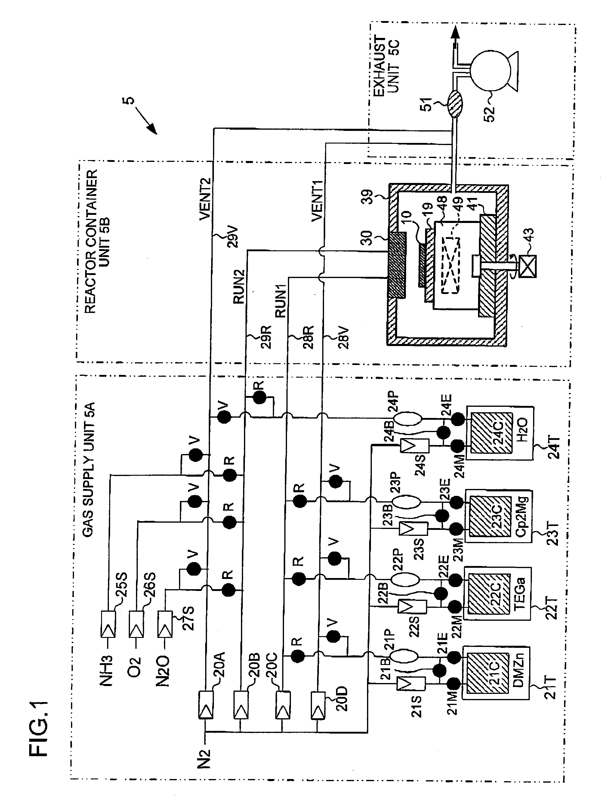
[0056]FIG. 1 schematically shows a configuration of an MOCVD apparatus 5 used for crystal growth. Particulars about an apparatus configuration of the MOCVD apparatus 5 will be described hereinafter. Further, a crystal growth material will be described later in detail.

[0057][Apparatus Configuration]

[0058]The MOCVD apparatus 5 inclu...

second embodiment

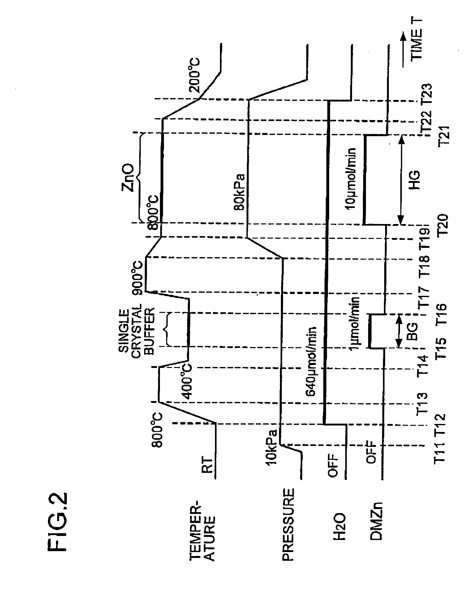
[0098]In this embodiment, a ZnO single crystal substrate was etched to remove deposits. A growth method including a growth material, a growth sequence (FIG. 2) and growth conditions is the same as that in the first embodiment except that the substrate was etched.

[0099]It is to be noted that a mixed solution obtained by mixing a solution containing 0.2 mol / L of EDTA·2Na (ethylene-diamine-tetra-acetic acid disodium salt) with a solution containing 99% of EDA (ethylene diamine) with a ratio of 20:1 was used as an etchant. An etching rate of this etchant (EDTA·2Na:EDA=20:1) is 0.7 μm / h. It is to be noted that the etchant is disclosed in Japanese Patent Application Laid-open No. 2007-1787. Further, a mixing ratio of the etchant is approximately 5:1 to 30:1, and etching can be excellently performed with this ratio.

[0100]The substrate was immersed in the etchant at a room temperature for 10 min (minutes) to etch a surface layer thereof. Then, the etchant was removed by water washing, and d...

third embodiment

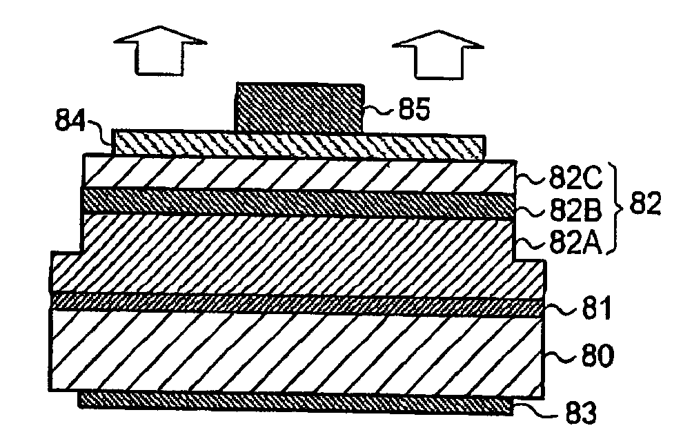
[0103]This embodiment is the same as the second embodiment except that a growth temperature of a buffer layer was set to 300° C. (Tbuf=300° C.). More specifically, water vapor (H2O) and the metalorganic compound containing no oxygen were used to grow a buffer layer 11C and a ZnO crystal 12C on a ZnO single crystal substrate 10 in which the substrate 10 was subjected to etching and a heat treatment (Tanl=800° C.). It is to be noted that the substrate having these growth layers formed thereon has the same layer structure as that in the second embodiment, and reference numerals in parentheses represent configurations of the buffer layer 11C and the ZnO crystal 12C of the third embodiment in a cross-sectional view (FIG. 4) showing the configuration of the second embodiment.

[0104]In more detail, the buffer layer 11C (a layer thickness is 25 nm) was formed based on low-temperature growth (Tbuf300° C.), and crystallinity of the buffer layer 11C was restored by annealing (Tcry=900° C.). Fur...


PUM


Abstract

A method which has a low-temperature growth step of growing a buffer layer of a ZnO-based single crystal on the substrate at a growth temperature in the range of 250° C. to 450° C. using a polar oxygen material and a metalorganic compound containing no oxygen; performing a heat treatment of the buffer layer to effect a transition of the buffer layer to a thermostable-state single crystal layer; and a high-temperature growth step of growing the ZnO-based single crystal layer on the thermostable-state single crystal layer at a growth temperature in the range of 600° C. to 900° C. using a polar oxygen material and a metalorganic compound containing no oxygen.

Description

BACKGROUND OF THE INVENTION[0001]1. Technical Field[0002]The present invention relates to a method for growing a zinc-oxide-based semiconductor device and a method for manufacturing a semiconductor device, and more particularly to a method for growing a zinc-oxide-based semiconductor layer on a ZnO substrate and a method for manufacturing a zinc-oxide-based semiconductor light emitting device based on an MOCVD method.[0003]2. Description of the Related Art[0004]A zinc oxide (ZnO) is a direct transition type semiconductor having band gap energy of 3.37 eV at a room temperature, and it is expected as a material for a photoelectronic device in a blue or ultraviolet region. In particular, it has physical properties very suitable for a semiconductor light emitting device, i.e., an exciton binding energy of 60 meV and a refractive index n=2.0. Further, the zinc oxide can be employed for a wide range of devices including surface-acoustic wave (SAW) devices, piezoelectric devices, and the l...

Claims


Application Information

Patent Timeline
IPC IPC(8): H01L33/28H01L21/36H01L29/22
CPCH01L21/02403H01L21/02472H01L2224/73265H01L2224/48247H01L2224/48091H01L21/02483H01L21/02554H01L21/02565H01L21/0262H01L29/22H01L33/0083H01L33/20H01L33/28H01L2224/45144H01L2924/13091H01L2224/32245H01L2924/00014H01L2924/00
Inventor HORIO, NAOCHIKAMAKISHIMA, MASAYUKI
Owner STANLEY ELECTRIC CO LTD
Why Eureka
Try Eureka