Method for Fabricating a Doped and/or Alloyed Semiconductor

a technology of alloyed semiconductors and semiconductor layers, which is applied in the direction of electrolysis components, vacuum evaporation coatings, coatings, etc., can solve the problems of low deposition rate of film preparation process, poor process reproducibility, and reduced optical transmission of materials, so as to achieve and facilitate the optimization of dopant concentration. , the effect of maintaining the desired structural, optical and electrical properties

Inactive Publication Date: 2010-12-23
NEW MILLENNIUM SOLAR EQUIP CORP
View PDF4 Cites 14 Cited by
  • Summary
  • Abstract
  • Description
  • Claims
  • Application Information

AI Technical Summary

Benefits of technology

[0008]What is needed is a deposition technique that can easily optimize the dopant concentration in a TCO, and while providing uniform dopant concentration over large surface area substrates, while maintaining the desired structural, optical and electrical properties. What is needed is a method that can readily provide doped and / or alloyed semiconductor layers using a single target material. The present invention provides a physical deposition process (i.e., sputtering) that is more flexible, more cost effective and less complicated than current deposition techniques. Specifically, the present invention permits in-situ composition control for doped and / or alloyed thin films, and permits facile control over varying the composition of doped and / or alloyed thin films that are used in multilayer devices. The present invention substantially reduces or eliminates the need for using multiple sputtering targets, or for designing and implementing sputtering targets having a doped composition, in order to deposit doped and / or alloyed films.

Problems solved by technology

However, at high dopant concentrations many materials suffer from reduced optical transmission due to increased light absorption (free carrier absorption) and impurity scattering.
While the constituent elements of ZnO are inexpensive, the film preparation process can suffer from low deposition rate, poor process reproducibility, poor uniformity and general unsuitability for large area coating.
Any combination of these drawbacks can lead to a high cost of the final ZnO thin film product.
The major problem with physical deposition techniques such as sputtering is the ability to variably control a dopant composition (e.g., for doping and / or alloying).
Specifically, doping and / or alloying of materials deposited by sputtering requires complex and cumbersome target preparation that typically requires several elements or compounds to be mixed and formed into a target having a fixed composition.
Thus, sputtering processes are not sufficiently flexible to be cost effective for applications that require the deposition of multiple layers having variable compositions or that require adjustments to be made to the composition of a layer to satisfy properties demanded of the layer.

Method used


Image

  • Method for Fabricating a Doped and/or Alloyed Semiconductor
  • Method for Fabricating a Doped and/or Alloyed Semiconductor
  • Method for Fabricating a Doped and/or Alloyed Semiconductor

Examples


example 1

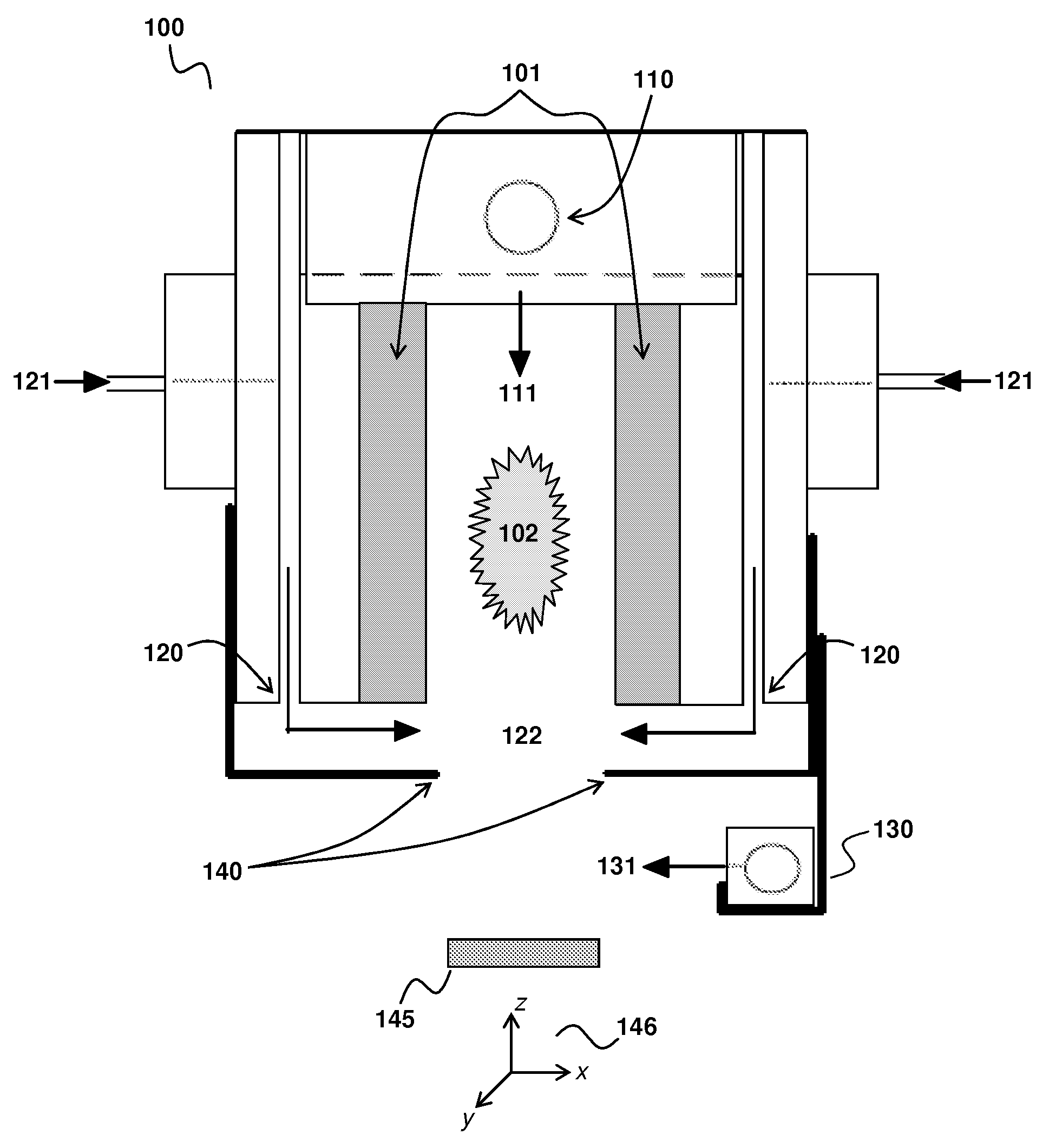
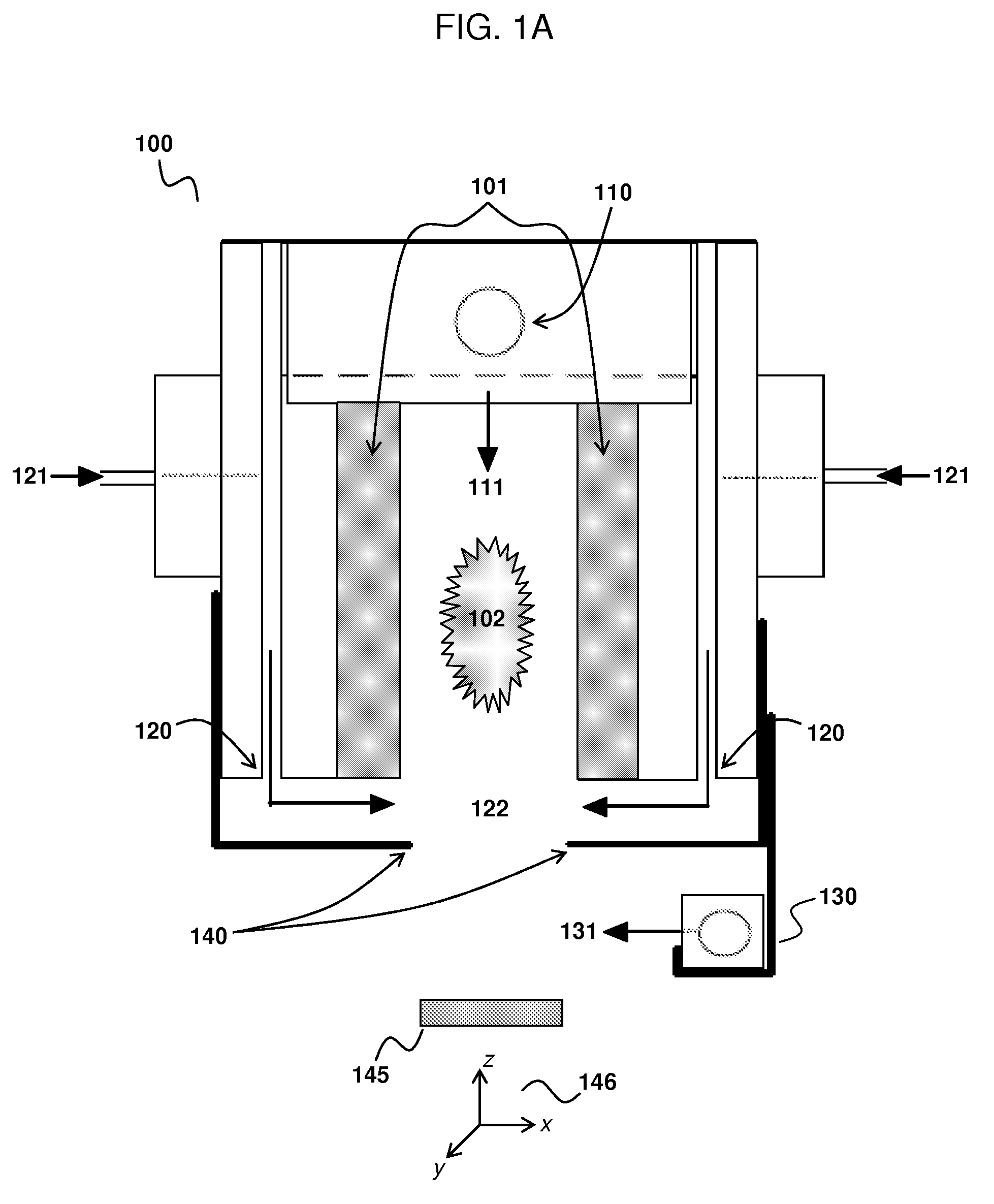
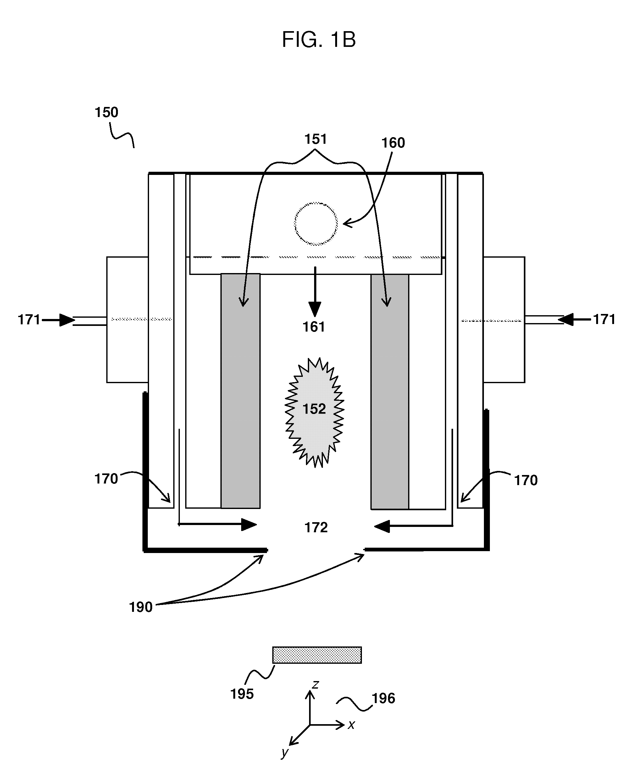
[0143]Zinc oxide (ZnO) and gallium-doped zinc oxide (GZO) films were deposited on glass substrates by a method of the present invention using an apparatus depicted in FIGS. 1-3. A zinc sputtering target was utilized for all depositions. An argon plasma was generated in the hollow cathode portion of the apparatus (the length of the cathode was about 15 cm), and an oxidant (O2) was introduced into the deposition chamber. Sputtered zinc was carried to the substrate and mixed with the oxidant by the argon flow. For the GZO films the metalorganic was triethylgallium (TEGa), which was introduced in the deposition chamber using argon as a carrier gas. The metalorganic TEGa was dissociated by the argon plasma and carried onto the substrate where it was co-deposited with the zinc oxide. The deposition conditions are outlined in the Tables below.

TABLESDeposition conditions and flow rates for undoped ZnO and GZO layers(deposited using a hollow cathode assemblyhaving a length of about 15 cm) . ...

example 2

[0145]The composition of the ZnO film and GZO films prepared in Example 1 was characterized using inductively coupled plasma optical emission spectrometry (ICP-OES). The results are presented in the Table below.

TABLEICP measurements of ZnO and GZO films.GaGa(403.298)(417.206)Zn (202.551)Zn (206.200)Sampleppmppmppmppm% GaStandard10.0010.0010.0010.00—Blank0.000.000.000.00—598−0.050.063187.31190.92  0%59921.5423.73583.07675.553.27%5976.176.09159.88157.023.63%594b30.7829.17327.17390.987.84%

[0146]Referring to the above Table, gallium concentrations of about 3.3% to about 7.8% were obtained. The gallium concentration of the GZO films can be correlated with the flow rate of argon and TEGa into the deposition chamber, as well as the TEGa bubbler temperature and pressure.

example 3

[0147]The compositional uniformity of the ZnO film and GZO films prepared in Example 1 was characterized using dynamic Secondary Ion Mass Spectrometry (d-SIMS). The depth profiles obtained from the d-SIMS analysis are presented graphically in FIGS. 4A-4B, 5A-5B and 6A-6B.

[0148]The depth profile for the undoped ZnO layer is provided in FIGS. 4A-4B. Referring to FIG. 4A, the depth profile for zinc, sodium and gallium in the ZnO layer indicates that the ZnO layer is free from gallium (i.e., gallium is below the detection limit), and substantially uniform with respect to the concentration of zinc. The sodium signature arises from the underlying glass substrate.

[0149]Referring to FIG. 4B, the depth profile for zinc+oxygen, fluorine, chlorine, hydrogen and carbon in the ZnO layer indicates that the ZnO film is substantially uniform with respect to zinc+oxygen, and substantially free of carbon. The ZnO film contains very low levels of the halides (i.e., F and Cl) and hydrogen.

[0150]The dep...


PUM

PropertyMeasurementUnit
refractive indexaaaaaaaaaa
distanceaaaaaaaaaa
temperatureaaaaaaaaaa

Abstract

The present invention is directed to methods for depositing doped and/or alloyed semiconductor layers, an apparatus suitable for the depositing, and products prepared therefrom.

Description

BACKGROUND OF THE INVENTION[0001]1. Field of the Invention[0002]The present invention relates to methods of depositing doped and / or alloyed semiconductor layers, an apparatus suitable for depositing doped and / or alloyed semiconductor layers, and products prepared therefrom.[0003]2. Background of the Invention[0004]Transparent Conductive Oxides (TCOs) are present in many consumer electronic devices and are a critical element for the development of high-efficiently photovoltaic devices. Applications for TCO thin films include transparent electrodes for flat panel displays, transparent electrodes for photovoltaic cells, low emissivity windows, window defrosters, transparent thin film transistors, light emitting diodes, semiconductor lasers, and the like. A TCO layer is often an integral part of thin-film solar cells, usually as a sun-facing (top) contact or as a back reflector in silicon-based solar cells. However, the usefulness of TCO thin films in solar cell applications depends str...

Claims


Application Information

Patent Timeline
Patent Type & Authority Applications(United States)
IPC IPC(8): H01L29/227H01L21/36C23C14/34C23C14/50H01L21/40
CPCC23C14/0057C23C14/086H01L21/02422H01L21/02631H01L21/02565H01L21/0262H01L21/02554
Inventor DELAHOY, ALAN E.SARAF, GAURAVGUO, SHEYU
Owner NEW MILLENNIUM SOLAR EQUIP CORP
Why Eureka
Try Eureka