

Method for electroconductive pattern formation
a technology of conductors and patterns, applied in the field of electroconductive pattern formation, can solve the problems of resist layer peeling or breaking, insufficient bonding strength of electrolytically plated copper, and large increase in production steps, so as to achieve easy production, easy dissolution or dispersion, and easy dissolution of photo-crosslinkable resin layers
- Summary
- Abstract
- Description
- Claims
- Application Information
AI Technical Summary
Benefits of technology
Problems solved by technology
Method used
Image

Examples
example 1
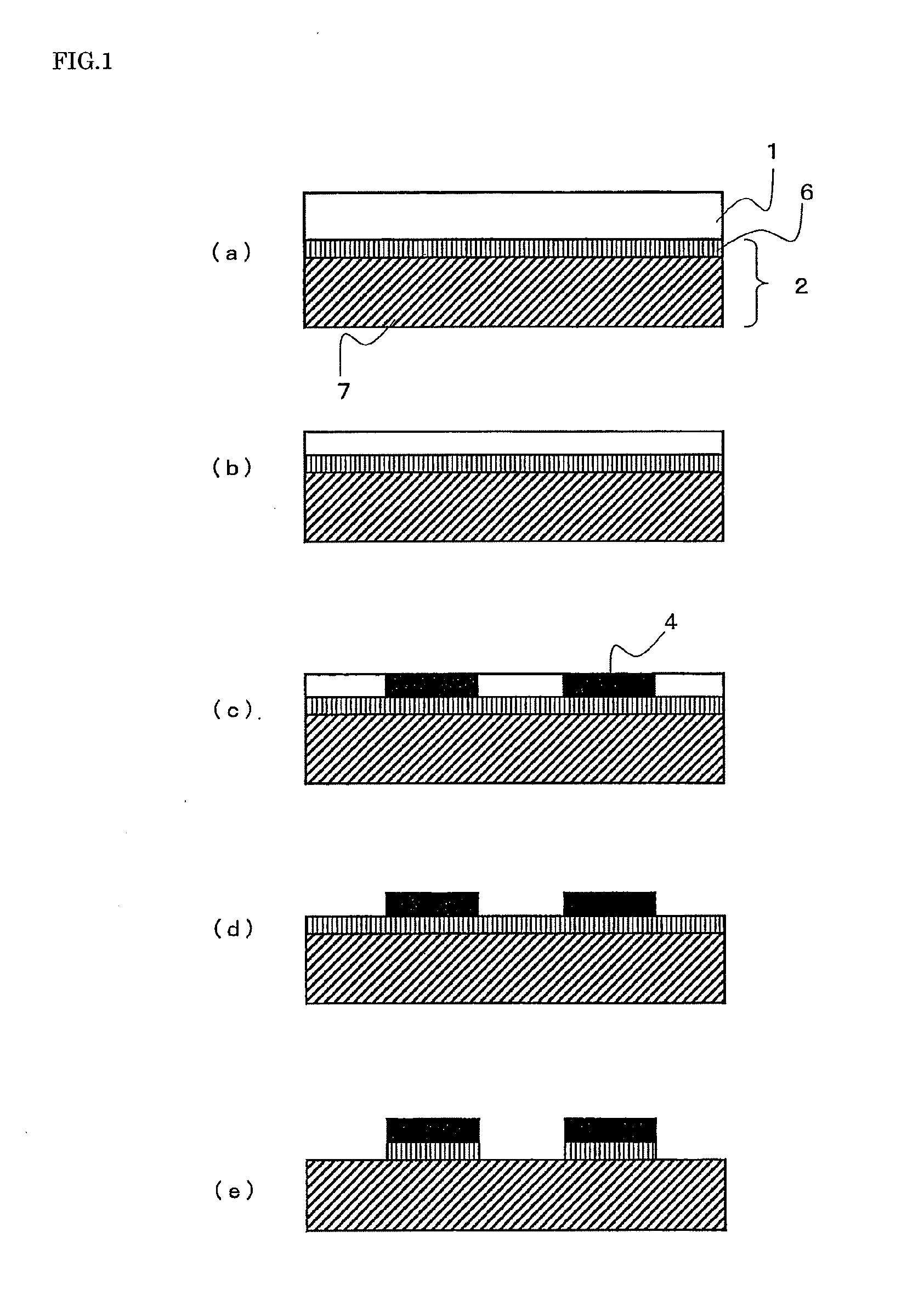
Step (a)
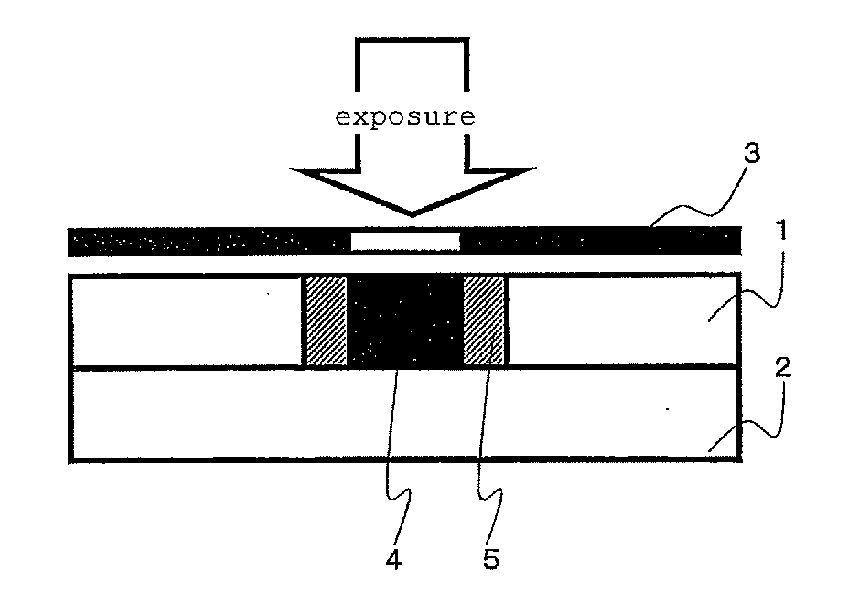
[0106]A dry film resist (trade name: Sunfort AQ2575, thickness 25 supplied by Asahi Kasei E-Materials) was laminated on an glass substrate epoxy resin copper-clad laminate (area 170 mm×255 mm, copper foil thickness 12 with, substrate thickness 0.1 mm, trade name: CCL-E170, supplied by Mitsubishi Gas Chemical Co., Inc.) by means of a dry film laminator having a laminating roll that was surface-treated for heat-resistant silicon rubber lining, with peeling off a protective film at a room temperature of 100° C. at an air supply pressure of 0.30 MPa and at a laminating speed of 0.50 m / minute.
Step (b)
[0107]After a supporting film was removed, the photo-crosslinkable resin layer was treated with an alkali aqueous solution A shown in Table 1 (liquid temperature 25° C., spray pressure 0.05 MPa) for a treatment time period shown in Table 2 such that the photo-crosslinkable resin layer had an average thickness of 10 μm, and it was fully washed with water and dried with cold air to giv...
examples 2-10
[0111]Conductor patterns were formed in the same manner as in Example 1 except that the alkali aqueous solution A was replaced with alkali aqueous solutions B to H, AH and AI described in Table 1. Each photo-crosslinkable resin layer after the treatment to render it thinner was measured for thicknesses in 10 points, and evaluated for thickness variability on the basis of values of the standard deviation G. Table 2 shows the results. In each of Examples 2 to 10, the value of the standard deviation was small, and good in-plane uniformity was obtained. Further, there were observed no defects of a broken line and a short circuit that would be a practical problem. In Examples 9 and 10 that used sodium sulfite as the inorganic alkaline compound, the photo-crosslinkable resin layers were good with regard to freedom from the in-plane variability of layer thickness, while on the surface of each photo-crosslinkable resin layer after the treatment to render them thinner was carried out, there ...
examples 11-28
[0114]Conductor patterns were formed in the same manner as in Example 1 except that the alkali aqueous solution was replaced with alkali aqueous solutions I to Z shown in Table 5 and that the treatments to render layers thinner were carried out by dipping photo-crosslinkable resin layers in the alkali aqueous solutions in addition to the spray treatment of ejecting alkali aqueous solutions at a spray pressure of 0.05 MPa, fully washing them with water and drying them by cold air. The dipping time periods and the spray ejecting time periods were adjusted such that the photo-crosslinkable resin layer after the treatments to render them thinner had an average thickness of 10 μm.
TABLE 5Amounts (part byAlkali aqueousmass (molarExamplesolutionComponentsconcentration))11Alkali aqueousSodium carbonate 5solution ISodium sulfite2 (0.17)Water9312Alkali aqueousSodium carbonate10solution JSodium sulfite2 (0.18)Water8813Alkali aqueousSodium carbonate15solution KSodium sulfite2 (0.19)Water8314Alka...
PUM
 Abstract
Description
Claims
Application Information