Functionalized fullerenes for nanolithography applications

a fullerene and nanolithography technology, applied in the field of nanolithography applications, can solve the problems of limited diffraction resolution, limited utility of pmma, and limited diffraction resolution

Inactive Publication Date: 2011-01-06
UNIV OF FLORIDA RES FOUNDATION INC
View PDF4 Cites 6 Cited by
  • Summary
  • Abstract
  • Description
  • Claims
  • Application Information

AI Technical Summary

Benefits of technology

[0017]The method allows for the direct development of the features of the resist immediately upon irradiation with the electron beam. No subsequent development step using a selective solvent is required to e

Problems solved by technology

When a “perfect” lens is used, the resolution of the features is said to be diffraction limited, where the minimum feature size attainable is limited only by the size of features in the mask where diffraction of the light projected through it occurs.
For direct-write applications, the electron beam can be delivered by a scanning electron microscope where resolution is not fixed by the diffraction limit, but rather resolution is limited primarily by the diameter to which the electron beam can be focused.
However, because the etch durability of P

Method used


Image

  • Functionalized fullerenes for nanolithography applications
  • Functionalized fullerenes for nanolithography applications
  • Functionalized fullerenes for nanolithography applications

Examples


example 1

[0032]A commercially available electron beam resist, (PMMA A2 950K in anisole; Microchem, Newton, Massachusetts) was purchased and a homogeneous solution was prepared by dissolving a functionalized fullerene, C60H18 to C60H20, at 0.1 weight % in the PMMA resist solution. This solution was spin coated on the surface of a silicon wafer resulting in a film with the approximate thickness of 200 nm. After the coating step, the wafer was baked in an oven at 190° C. for 45 minutes. A Raith-150 direct write electron beam lithography tool was employed for irradiation of a nanostructured pattern with an electron beam having a 10 kV accelerating voltage using software provided with the tool.

example 2

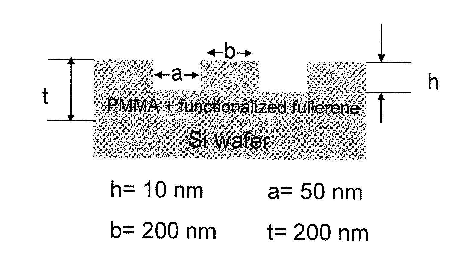
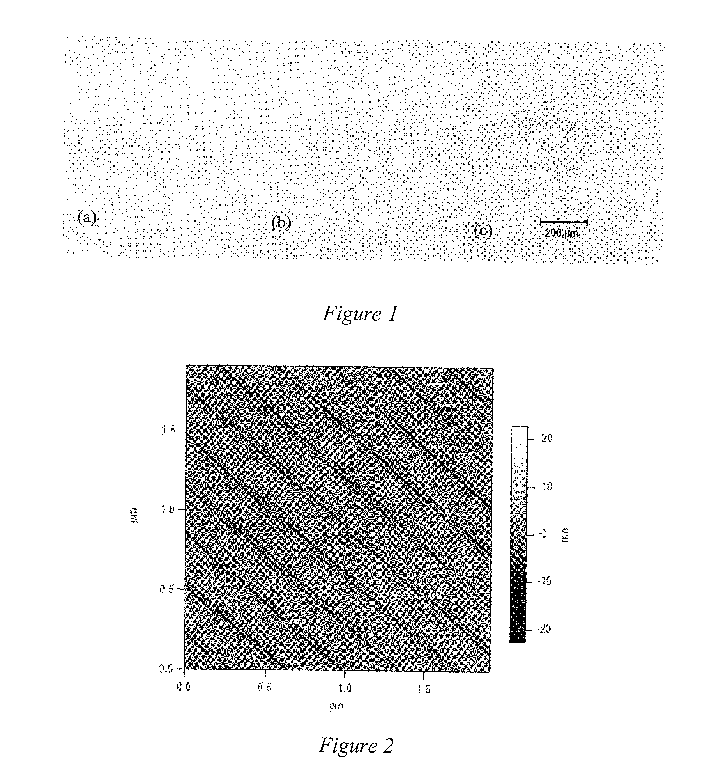
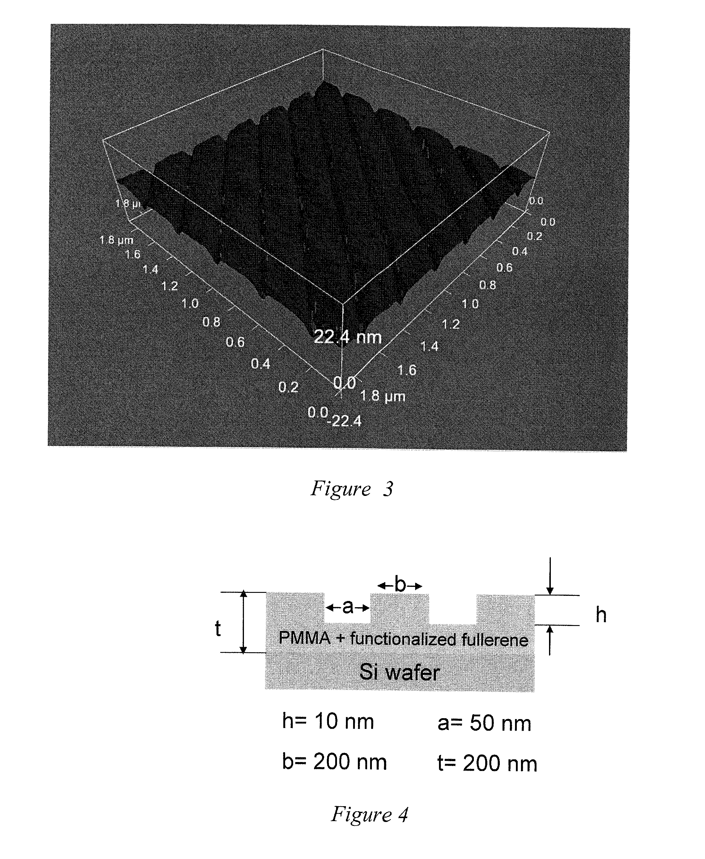
[0033]The electron beam exposed coated substrate of Example 1 was examined using an optical microscope and an Atomic Force Microscope (AFM). An optical image of the exposed wafer without any traditional development step is shown in FIG. 1. This image consists of 25 microns wide lines and 50×50 microns square. The square boxes contain additional features with nanometer dimensions. These square boxes were imaged with AFM. The AFM image of a portion of the box is displayed in FIG. 2. The lines have widths of approximately 50 nm. FIG. 3 is a three-dimensional image of the portion of the box displayed in FIG. 2 and shows that the depth of the lines is approximately 10 nm. A schematic is given in FIG. 4 of the patterned substrate of the boxes illustrating the approximate dimensions.


PUM


Abstract

A method for electron beam nanolithography without the need for development step involves depositing a film of a resist comprising functionalized fullerenes on a substrate, and writing features by exposure to an electron beam with an accelerating voltage and dose rate sufficient to promote heating or thermal degradation of the functionalized fullerene in the irradiated volume such that a pattern is generated without a subsequent development step or with an aqueous developer. Lithographic features of about 1 nm or greater can be formed.

Description

CROSS-REFERENCE TO RELATED APPLICATION(S)[0001]The present application claims the benefit of U.S. Provisional Application Ser. No. 61 / 010,169, filed Jan. 4, 2008, which is hereby incorporated by reference herein in its entirety, including any figures, tables, or drawings.BACKGROUND OF THE INVENTION[0002]The creation of well-defined micron-scale features upon a surface is the foundation of the microelectronics industry. Small features raise the efficiency of a microelectronic device and, ultimately, the ability to create smaller features drives advancement in the semiconductor industry. Photolithography has been the dominant method for fabrication of microcircuitry since the first semiconductor transistor circuit was developed. In a photolithography process, a monochromatic light is projected through a mask to create, generally after a development step, a pattern in a resist material supported on a substrate, generally a semiconductor. The patterned resist material protects portions ...

Claims


Application Information

Patent Timeline
IPC IPC(8): G03F7/20
CPCG03F7/039H01L21/0277G03F7/2059Y10S430/143
Inventor SINGH, AMIT KUMARKRISHNA, VIJAYMOUDGIL, BRIJ M.KOOPMAN, BENJAMIN L.
Owner UNIV OF FLORIDA RES FOUNDATION INC
Why Eureka
Try Eureka