Method for manufacturing electrodes of solar cell and electrochemical depositing apparatus

a technology of solar cells and electrodes, applied in the direction of electrolytic processes, semiconductor devices, electrolysis components, etc., can solve the problems of low conversion efficiency of the present commercial solar cell, short service life of the solution relatively slow chemical process of chemical depositing copper, etc., to save heating costs, facilitate production control, and widen the scope of operation

Inactive Publication Date: 2011-02-24
WUXI SUNTECH POWER CO LTD
View PDF8 Cites 16 Cited by
  • Summary
  • Abstract
  • Description
  • Claims
  • Application Information

AI Technical Summary

Benefits of technology

[0020]Owing to the fact that the principle of chemical depositing metal and that of electrochemical depositing metal are fundamentally different, the rate of formation of the electrodes of the invention, namely, the rate of depositing metal is much faster than the rate of chemical depositing metal. An important advantage of the present invention is that the time of formation of the electrodes is decreased from approximately 10 hours for chemical depositing metal to within an hour. Generally, the formation of the electrodes may be completed in more than 10 minutes.
[0021]Another advantage of the present invention is that because the process of electrochemical depositing metal is simpler than that of chemical depositing metal, the scope of operation is wider, and thus electrochemical depositing metal is particularly appropriate for industrial production. For example, the temperature required by electrochemical depositing metal is not high, and electrochemical depositing metal may be generally operated at room temperature, thus, it is not only convenient for control of production, but also saves the heating cost. The composition of the electrolytic solution used in the process of electrochemical depositing is also very simple, and accordingly, the electrolytic solution may be used repeatedly for a long time.
[0022]The metal electrodes formed in a general process of chemical depositing are not crystalline, while the metal electrodes of electrochemical depositing are crystallitic, accordingly, the metal electrodes formed by electrochemically deposited have better stability and conductivity, which directly influences that the metal electrodes of electrochemical depositing can reduce the loss of current produced by the solar cell on the electrodes and improve the conversion efficiency of solar cell.
[0023]Because the chemical reaction of electrochemical depositing metal is very simple, for example, influences of electrochemical depositing metal on PH value of electrolytic solution and change in the composition of the solution are very little, and the management of the solution is also very simple, the process of electrochemical depositing of the present invention is appropriate for industrial production. More importantly, the manufacture cost for the method in formation of the electrodes of solar cell of the present invention is very low. And the treatment for waste liquid is simpler than chemical depositing metal. For the solar cell produced by the electrochemical process according to the present invention, there is little waste liquid, and the treatment of waste liquid is easy to be made.

Problems solved by technology

Such design of solar cell is one of the reasons why the conversion efficiency of the present commercial solar cell is low.
The process of chemical depositing copper is a relatively slow chemical process, which generally needs approximately 10 hours to obtain a required thickness of copper electrodes.
Another problem of manufacturing the electrodes of the buried contact cell by using the method for chemical depositing copper is that the service life of the solution of chemical depositing copper is short, wherein the solution cannot be used any more after being used for several batches.
Because the organics that is difficult for process are contained in the discharged waste liquid, the process using chemical depositing copper increases the production cost.
Additionally, the solution of chemical depositing copper is relatively unstable, and the self-precipitation of copper easily occurred, which influences the normal production.
In addition, most of the operations processes for chemical depositing copper are performed at a temperature which is higher than the room temperature, for example, higher than 50 degree, and thus a great amount of energy supply is required for such a process, and the production cost is further increased.
Due to the long period of the reaction time, the energy consumption is quite considerable.
The problem that how to overcome the disadvantages of the conventional technology described above while improving the photoelectric conversion efficiency needs to be overcome urgently.

Method used


Image

  • Method for manufacturing electrodes of solar cell and electrochemical depositing apparatus
  • Method for manufacturing electrodes of solar cell and electrochemical depositing apparatus
  • Method for manufacturing electrodes of solar cell and electrochemical depositing apparatus

Examples


first embodiment

The First Embodiment

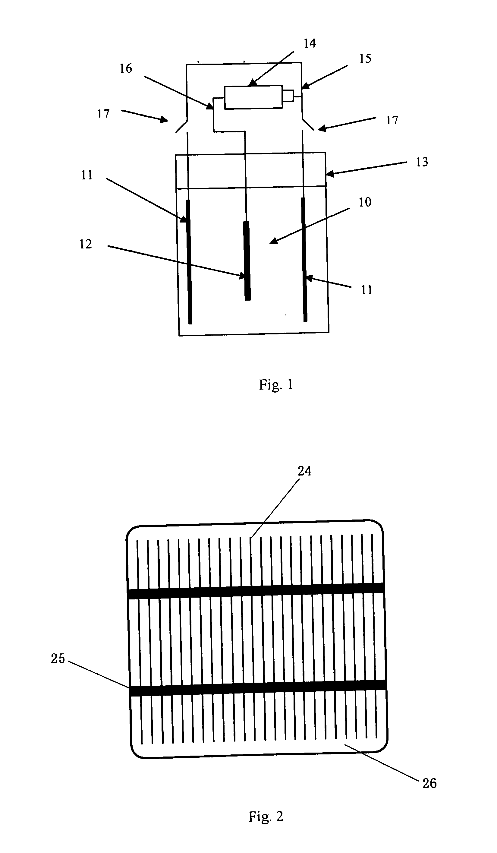
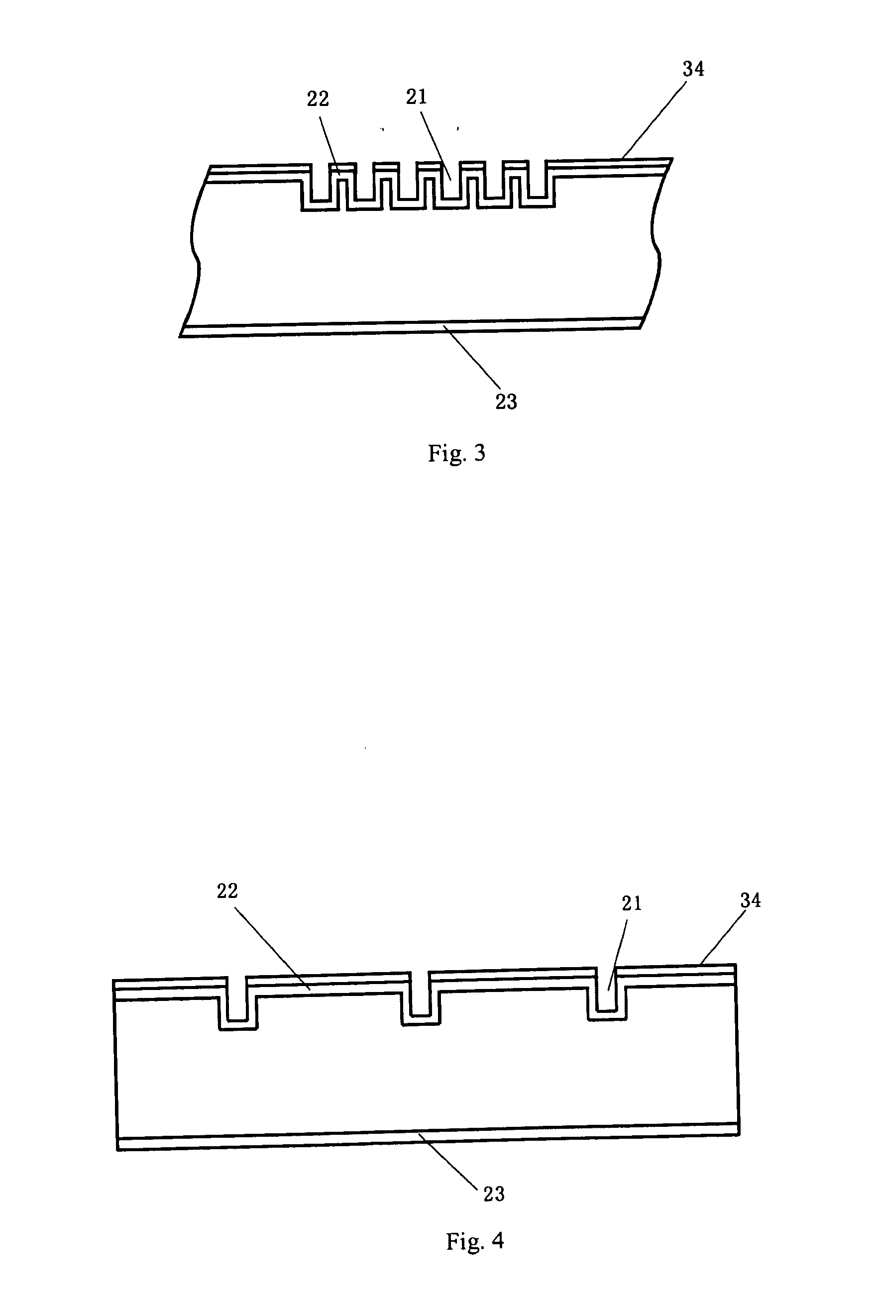
[0048]Shallowly diffusion is performed to a 125*125 mm sheet of monocrystalline silicon after it being washed and textured; the sheet resistance of the emitter 22 shallowly diffused is controlled to 150Ω; a layer of silicon nitride is deposited on the surface of the emitter 22 as passivation and antireflection film 34. Grooves 21 are fluted on the surface of the emitter 22 by the laser to form main gratings 25 and auxiliary gratings 24 crossing each other; a deep diffusion is performed to the main gratings 25 and auxiliary gratings 24 after they are washed so that the sheet resistances of the main gratings 25 and auxiliary gratings 24 achieve to 10Ω below; aluminum is sputtered on the back of the emitter 22 and sintered to form an aluminum back surface field i.e., back electrode 23; a chemical depositing nickel treatment is made to the silicon sheet on which the aluminum back surface field is formed after the said silicon sheet is rinsed by hydrofluoric acid, aft...

second embodiment

The Second Embodiment

[0061]Diffusion is performed to a 125*125 mm sheet of polycrystalline silicon to form a PN Junction after the damage layer of the sheet of polycrystalline silicon is washed; the sheet resistance after diffused is 100Ω. Then a film of silicon nitride is deposited on the surface of the emitter of the polycrystalline silicon for passivation and antireflection. The silicon nitride at the main grating 25 and auxiliary gratings 24 is eroded to clean by using the method of chemical erosion, and then the deep diffusion is performed so that the sheet resistance at the grating part is below 10Ω. Aluminum is screen printed on the back of the emitter 22 and sintered to form an aluminum back surface field i.e., back electrode 23. Then depositing a layer of thin film of nickel by dipping the polycrystalline silicon in the solution in which nickel is chemical deposited, a nickel alloy is formed after sintering, then a electrochemical deposition treatment is made to the polycry...

third embodiment

The Third Embodiment

[0066]It is proved that the photoelectric conversion efficiency of solar cell achieved by depositing a layer of metal on the main gratings and auxiliary gratings of the emitter by using the method of chemical depositing metal firstly to reduce the resistance of the gratings, and then electrochemical depositing.

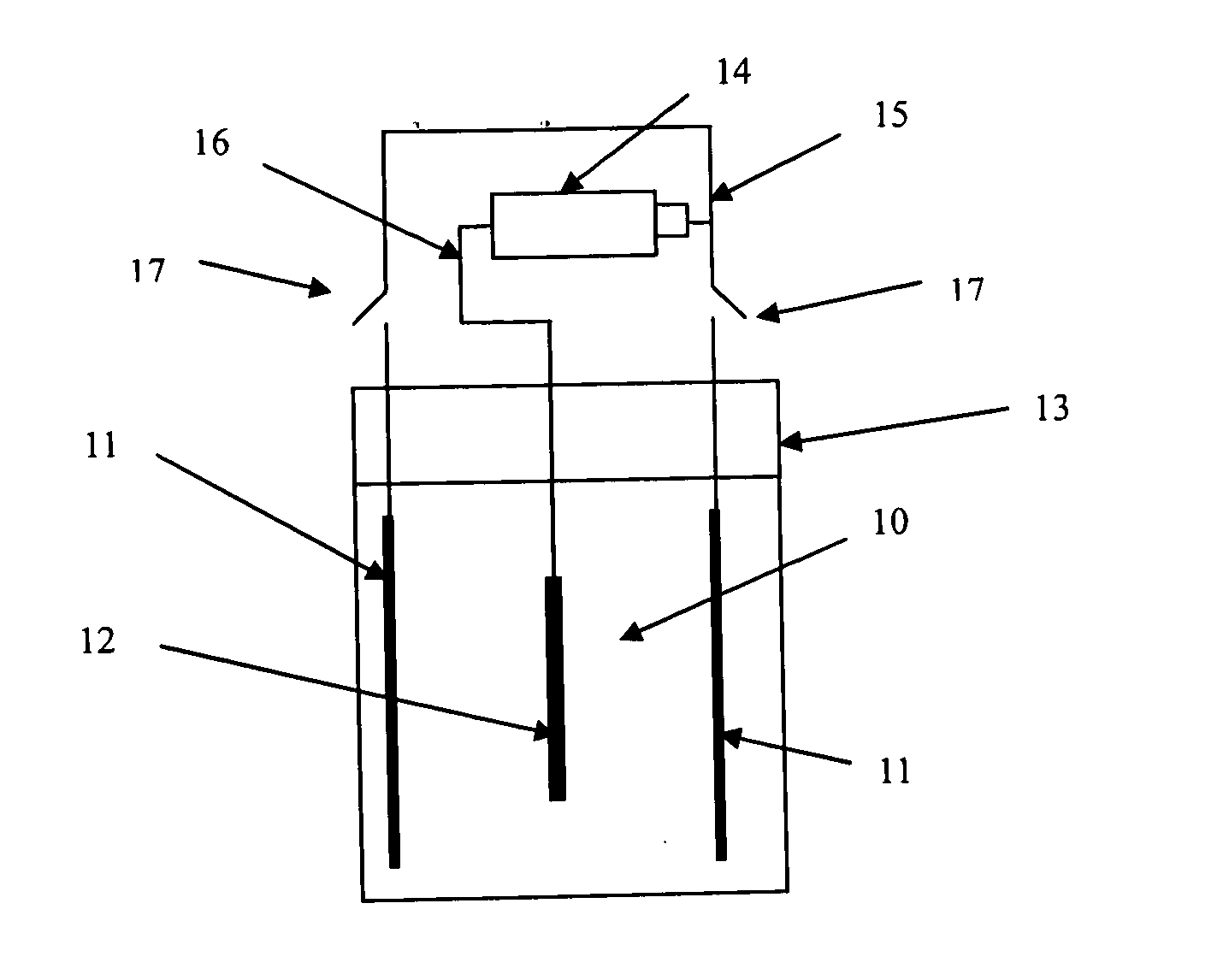
[0067]Specifically, after forming the silicon and nickel alloy by sintering the silicon sheet with the aluminum back surface field of the second embodiment, after chemical depositing copper for about 15 min, the resistance of the auxiliary gratings are at 1Ω per centimeter, then the negative electrode of the pulse power is connected to one side of the main grating and disposed in the electrolytic bath 13, in which the electrolytic solution 10 is the bluestone solution, and the two sides of the silicon sheet are the copper board which connected to the positive electrode of the pulse power, and the current concentration is controlled at 2.5 ampere per decimet...


PUM

PropertyMeasurementUnit
widthaaaaaaaaaa
timeaaaaaaaaaa
timeaaaaaaaaaa

Abstract

A method for manufacturing electrodes of solar cell and electrochemical depositing apparatus are disclosed. The method for manufacturing electrodes of solar cell is a method using the process of electrochemical depositing metal or metal alloy to form electrodes of solar cell. The method of the present invention can improve photoelectric conversion efficiency and reduce the production cost. The reaction time of the method is short and industrial waste liquid is treated easily.

Description

FIELD OF THE INVENTION[0001]The present invention relates to a method for manufacturing electrodes of solar cell and electrochemical depositing apparatus. More specifically, the present invention relates to a method for manufacturing electrodes of solar cell and electrochemical depositing apparatus, which can improve photoelectric conversion efficiency and reduce the production cost. The reaction time of the method is short and the industrial waste liquid produced can be treated easily.BACKGROUND OF THE INVENTION[0002]Solar cell is an apparatus that can convert the light energy into electric energy. Generally, the solar cell may include film solar cell and semiconductor slice solar cell such as the crystalline silicon solar cell in the semiconductor slice solar cell may include monocrystalline silicon solar cell and polycrystalline silicon solar cell. The conversion efficiency of solar cell for converting the energy of sunlight into electric energy is an important performance for th...

Claims


Application Information

Patent Timeline
Patent Type & Authority Applications(United States)
IPC IPC(8): H01L31/18C25D19/00
CPCC25D5/18C25D17/00H01L31/022425C25D7/12Y02E10/52C25D17/001H01L31/18Y02E10/50C25D5/611C25D7/126H01L31/04H01L31/0224
Inventor JI, JINGJIASHI, ZHENGRONGQIN, YUSENWENHAM, STUARTARTES, GRAHAM
Owner WUXI SUNTECH POWER CO LTD
Why Eureka
Try Eureka