Semiconductor apparatus and manufacturing method thereof

a technology of semiconductor devices and manufacturing methods, which is applied in the direction of semiconductor devices, electrical devices, transistors, etc., can solve the problems of high cost due to increase in the number of process steps, low transconductance (hereinafter referred to as “gm”), and deterioration of flicker-noise characteristics, so as to reduce leakage current, reduce the strength of electric fields, and reduce the effect of electric field strength

Inactive Publication Date: 2011-06-02
PANASONIC CORP
View PDF5 Cites 19 Cited by
  • Summary
  • Abstract
  • Description
  • Claims
  • Application Information

AI Technical Summary

Benefits of technology

[0030](1) According to the semiconductor apparatus of the present invention, the impurity diffusion area, which is to be the emitter area, is formed such that a low impurity density emitter diffusion layer is formed in the circumference of the emitter area near the upper surface thereof. With this structure, the electric field strength, which occurs at the emitter-base junction, is lowered, and the leakage current is reduced when a reverse voltage is applied between the emitter and the base.
[0031]Also, since it lowers the strength of the electric field that occurs at the emitter-base junction, the structure can restrict the reduction of hFE that occurs when carriers, which have been accelerated by the electric field that occurs at the emitter-base junction, collide with the insulation film on the upper surface to cause a defect (trap level or the like) to occur, when a reverse voltage is applied between the emitter and the base, and thus the range of the reverse voltage between the emitter and the base can be extended.
[0032]Since the low impurity density portion occupies a smaller portion of the emitter diffusion layer than the high impurity density emitter diffusion layer, the reduction in hFE caused by reduction in the emitter Gummel number (impurity density×thickness of emitter diffusion layer) is on the level of no problem. Furthermore, since there is a low impurity density second emitter area in the circumference of the emitter, the junction capacitance between the emitter and the base is also reduced, and “ft” of the bipolar transistor is improved. In addition, since there is no change in the junction depth of the emitter diffusion layer or the width in the depth direction of the base area (base width), the breakdown voltage between the collector and the emitter is not reduced.
[0033]Also, even in the case where the emitter diffusion layer is made shallow in order to improve the high-frequency characteristics of the bipolar transistor, according to the above-described structure, the low impurity density emitter diffusion layer is present under the conductive film. This structure prevents the emitter electrode from being arranged in the vicinity of the emitter-base junction, and reduces the leakage current between the emitter and the base.
[0034]Furthermore, even if the metal silicide is formed in the emitter diffusion layer to reduce the parasitic resistance of the emitter diffusion layer, the metal silicide can be separated from the emitter-base junction by a sufficient distance, making it possible to reduce the leakage current between the emitter and the base.
[0035]Furthermore, since, in this structure, the strength of the electric field, which occurs at the emitter-base junction, is lowered in the vicinity of the surface of the emitter diffusion layer, the ESD tolerance is improved when the surge voltage is applied to the emitter.

Problems solved by technology

The MOS transistor, however, has a defect that the transconductance (hereinafter referred to as “gm”) is low compared with the bipolar transistor.
This makes the current susceptible to the effect of the crystal lattice defect that exists on the surface of the semiconductor substrate, flicker-noise characteristic (also referred to as “1 / f noise characteristic”) is deteriorated compared with the bipolar transistor.
Furthermore, the MOS transistor is inferior than the bipolar transistor in the mismatch characteristic (difference between threshold voltages of the pair transistor) which is an important factor in the analog circuit.
However, when a bipolar transistor is loaded in the CMOS process used in the digital circuit, the following problems arise: high cost due to increase in the number of process steps; deterioration in the characteristic of the MOS transistor due to addition of thermal process or processing process for forming the bipolar transistor; and high cost due to increase in chip area (this problem arises because the bipolar transistor is larger in area than the MOS transistor).

Method used


Image

  • Semiconductor apparatus and manufacturing method thereof
  • Semiconductor apparatus and manufacturing method thereof
  • Semiconductor apparatus and manufacturing method thereof

Examples


first embodiment

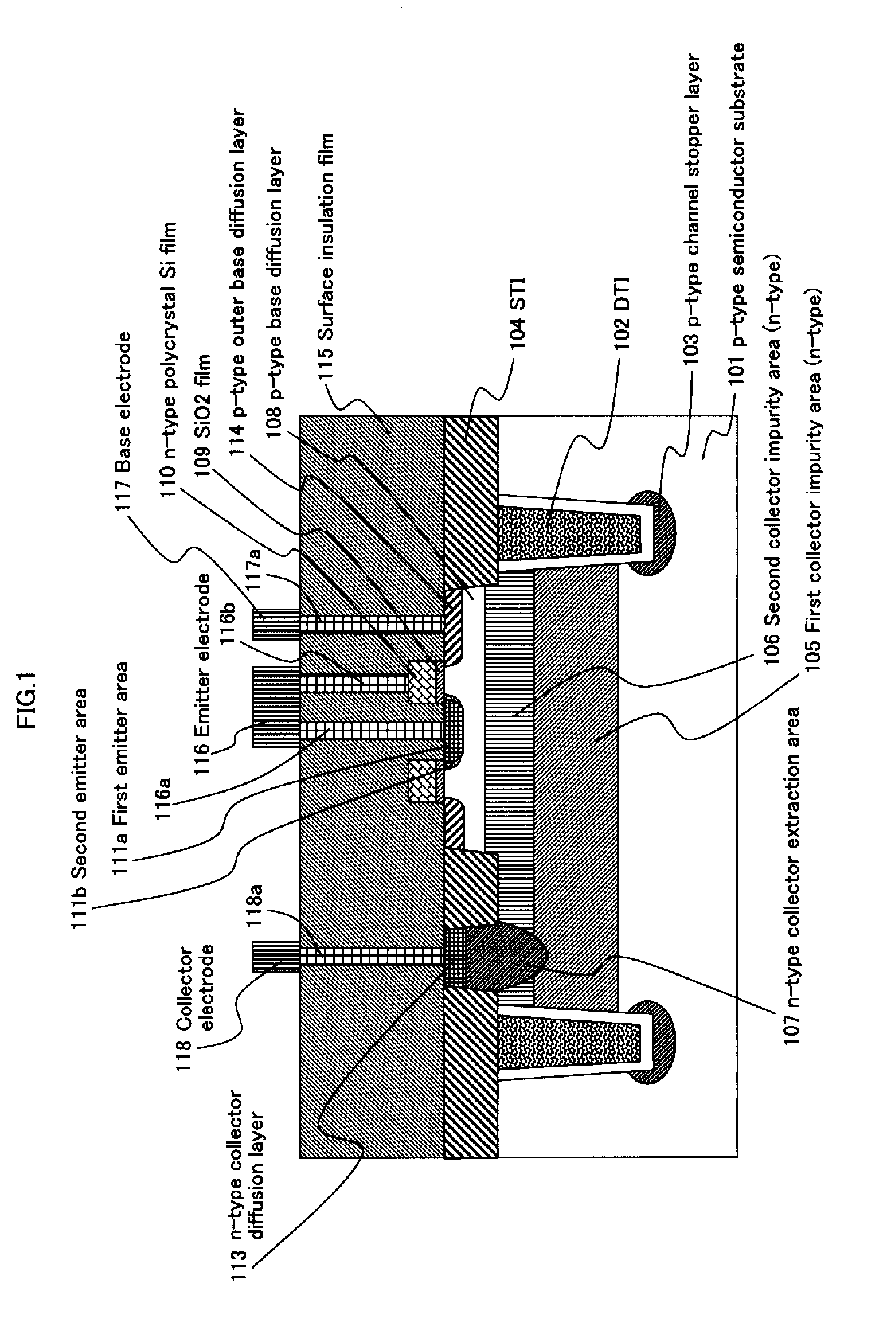
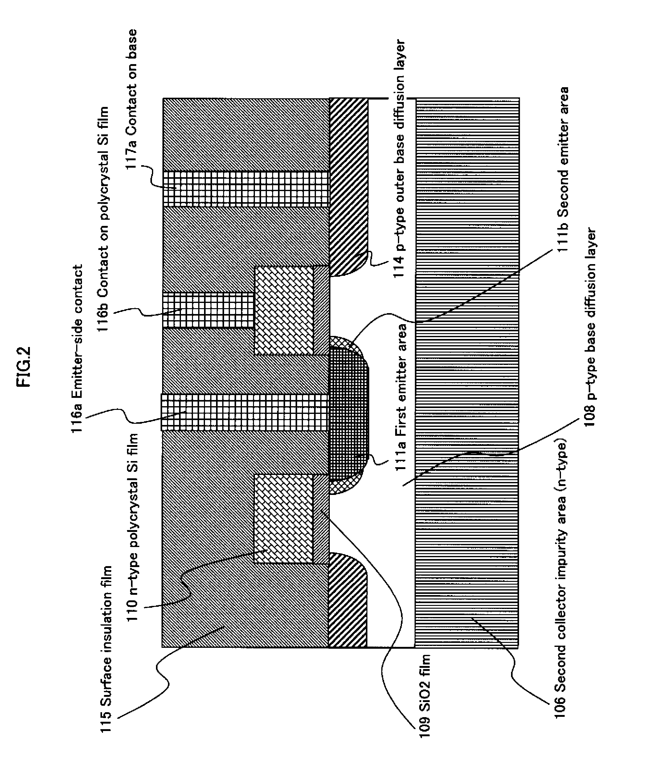
[0097]The following describes a semiconductor apparatus and a manufacturing method thereof in the first embodiment of the present invention with reference to the attached drawings. FIG. 1 is a cross-sectional view showing the semiconductor apparatus in the first embodiment of the present invention. FIGS. 2 through 6 are cross-sectional views showing manufacturing steps of the semiconductor apparatus in the first embodiment shown in FIG. 1. Note that the first embodiment may be referred to as Embodiment 1 as well.

[0098]FIGS. 1 through 6 are cross-sectional views showing a vertical-type NPN bipolar transistor contained in the semiconductor apparatus and manufacturing steps thereof.

[0099]As shown in FIG. 1, in a p-type semiconductor substrate 101 composed of a silicon substrate, a deep trench isolation (DTI) 102 and a shallow trench isolation (STI) 104 are formed as a device separation area for separating the bipolar transistor from the other devices. A p-type channel stopper layer 103...

modification 1

[Modification 1]

[0156]The following describes a modification of the semiconductor apparatus and manufacturing method thereof in the first embodiment of the present invention with reference to the attached drawings. FIG. 8 is a cross-sectional view showing the semiconductor apparatus in the present modification. FIGS. 9 through 10 are cross-sectional views showing manufacturing steps of the semiconductor apparatus shown in FIG. 8. Note that the portions that are the same as the structural portions having been explained with reference to FIGS. 1 through 7 are attached the same reference signs and description thereof is omitted.

[0157]FIGS. 8 through 10 are cross-sectional views showing a vertical-type NPN bipolar transistor contained in the semiconductor apparatus of the present modification and manufacturing steps thereof.

[0158]As shown in FIG. 8, a side wall 125 made of an insulation film is formed on the sides of the n-type polycrystal Si film 110 which is provided on a ring-like Si...

modification 2

[Modification 2]

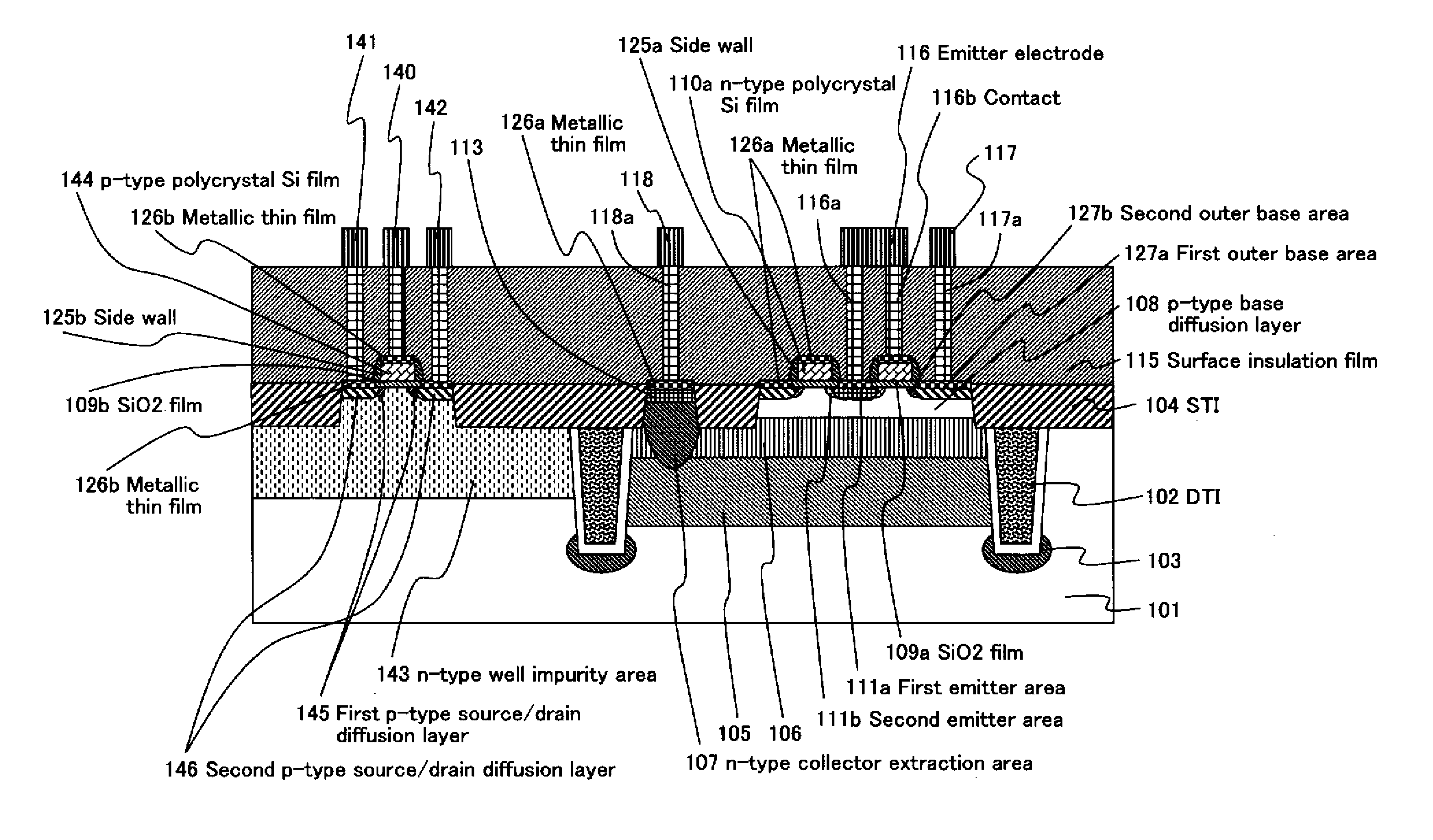
[0172]The following describes another modification of the first embodiment of the present invention with reference to the attached drawings. FIG. 11 is a cross-sectional view showing the semiconductor apparatus in Modification 2 of the present invention. FIG. 12 is a cross-sectional view showing a manufacturing step of the semiconductor apparatus shown in FIG. 11. Note that the portions that are the same as the structural portions having been explained with reference to FIGS. 1 through 10 are attached the same reference signs and description thereof is omitted.

[0173]FIGS. 11 through 12 are cross-sectional views showing a vertical-type NPN bipolar transistor contained in the semiconductor apparatus and manufacturing steps thereof.

[0174]The structure shown in FIG. 11 is different from the structure shown in FIG. 8 in that a metallic thin film 126 (hereinafter also referred to as “metal silicide”) is formed on an upper surface of each of the ring-like n-type polycrystal...


PUM


Abstract

A high-performance semiconductor apparatus which can be easily introduced into the MOS process, reduces the leakage current (electric field strength) between the emitter and the base, and is insusceptible to noise or surge voltage, and a manufacturing method of the semiconductor apparatus. The emitter 111 is formed by performing the ion implantation twice by using the conductive film (109) as a mask. The second emitter area (111b) is formed by ion implantation of a low impurity density impurity ion, and the first emitter area (111a) is formed by ion implantation of a high impurity density impurity ion. As a result, the low impurity density second emitter area is formed in the circumference of the emitter 111, which lowers the electric field strength, and reduces the leakage current. Also the conductive film is connected with the emitter electrode (116), which makes the apparatus insusceptible to noise.

Description

[0001]The disclosure of Japanese Patent Application No. 2009-273525 filed Dec. 1, 2009 including specification, drawings and claims is incorporated herein by reference in its entirety. Also, applications cited in the text of the present application, documents or references cited in the applications, and documents or references cited in the documents or references are incorporated herein by reference in the present application. The documents and the like incorporated in the present application may be used for implementing the present invention.BACKGROUND OF THE INVENTION[0002]1. Field of the Invention[0003]The present invention relates to a semiconductor apparatus and a manufacturing method thereof, in particular to a high-performance, low-cost bipolar transistor for use in a BiMOS or BiCMOS circuit, and a manufacturing method thereof.[0004]2. Description of the Related Art[0005]In recent years, as the integration and functionality of the semiconductor integrated circuit becomes high...

Claims


Application Information

Patent Timeline
Patent Type & Authority Applications(United States)
IPC IPC(8): H01L27/06H01L21/8249
CPCH01L21/8249H01L27/0623H01L29/0804H01L29/7325H01L29/402H01L29/66272H01L29/1004
Inventor TANAKA, MITSUO
Owner PANASONIC CORP
Why Eureka
Try Eureka