Eureka AIR delivers breakthrough ideas for toughest innovation challenges, trusted by R&D personnel around the world.

Antireflective Coating Composition and Process Thereof

a technology of coating composition and anti-reflective coating, applied in the direction of photosensitive materials, instruments, photomechanical equipment, etc., can solve the problems of back reflectivity, thin film interference effect and reflective notching, and change in critical line width dimensions

Active Publication Date: 2011-06-23
MERCK PATENT GMBH
View PDF62 Cites 13 Cited by
  • Summary
  • Abstract
  • Description
  • Claims
  • Application Information

AI Technical Summary

Benefits of technology

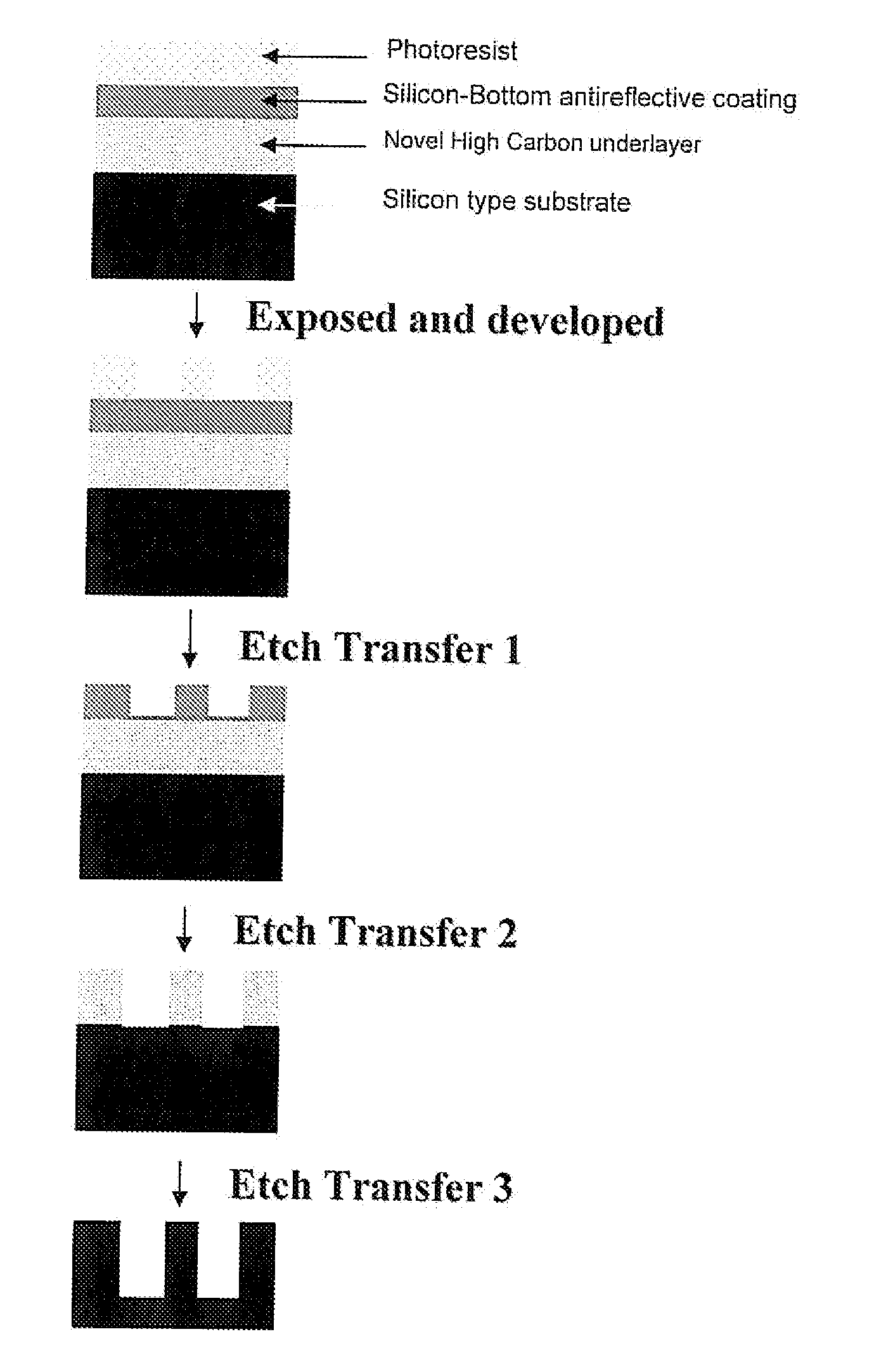
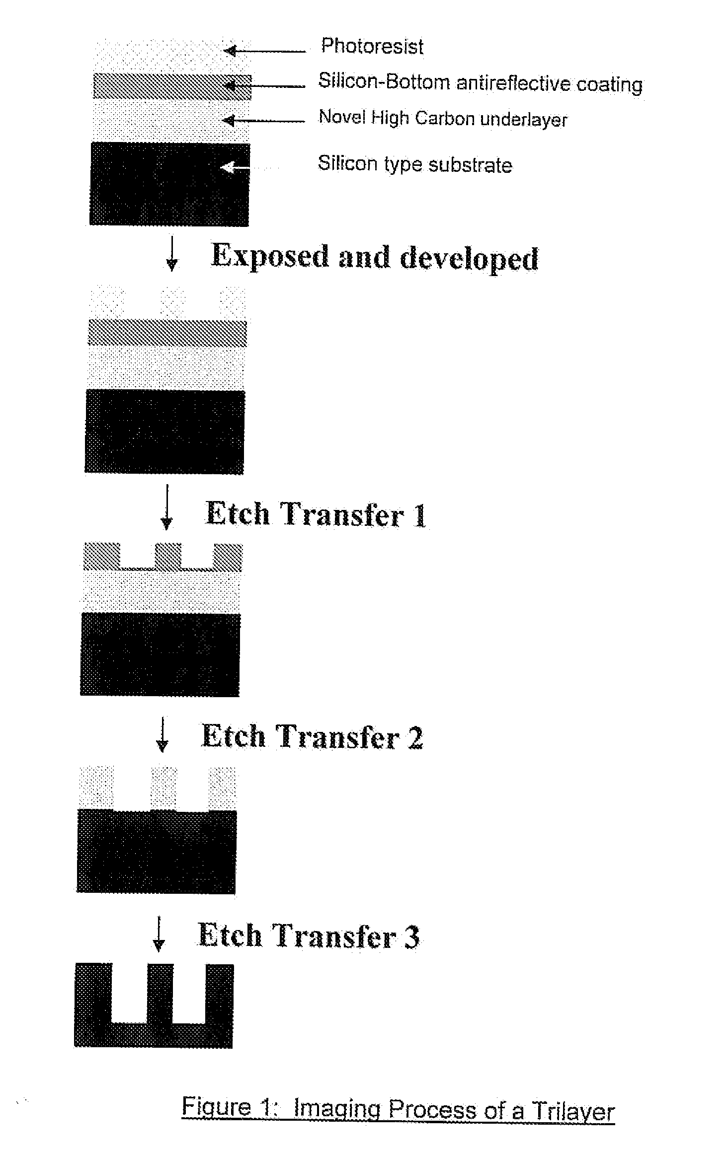
[0005]Absorbing antireflective coatings and underlayers in photolithography are used to diminish problems that result from back reflection of light from highly reflective substrates. Two major disadvantages of back reflectivity are thin film interference effects and reflective notching. Thin film interference, or standing waves, result in changes in critical line width dimensions caused by variations in the total light intensity in the photoresist film as the thickness of the photoresist changes or interference of reflected and incident exposure radiation can cause standing wave effects that distort the uniformity of the radiation through the thickness. Reflective notching becomes severe as the photoresist is patterned over reflective substrates containing topographical features, which scatter light through the photoresist film, leading to line width variations, and in the extreme case, forming regions with complete photoresist loss. An antireflective coating coated beneath a photoresist and above a reflective substrate provides significant improvement in lithographic performance of the photoresist. Typically, the bottom antireflective coating is applied on the substrate and then a layer of photoresist is applied on top of the antireflective coating. The antireflective coating is cured to prevent intermixing between the antireflective coating and the photoresist. The photoresist is exposed imagewise and developed. The antireflective coating in the exposed area is then typically dry etched using various etching gases, and the photoresist pattern is thus transferred to the substrate. Multiple antireflective layers and underlayers are being used in new lithographic techniques. In cases where the photoresist does not provide sufficient dry etch resistance, underlayers or antireflective coatings for the photoresist that act as a hard mask and are highly etch resistant during substrate etching are preferred, and one approach has been to incorporate silicon into a layer beneath the organic photoresist layer. Additionally, another high carbon content antireflective or mask layer is added beneath the silicon antireflective layer, which is used to improve the lithographic performance of the imaging process. The silicon layer may be spin coatable or deposited by chemical vapor deposition. Silicon is highly etch resistant in processes where O2 etching is used, and by providing a organic mask layer with high carbon content beneath the silicon antireflective layer, a very large aspect ratio can be obtained. Thus, the organic high carbon mask layer can be much thicker than the photoresist or silicon layer above it. The organic mask layer can be used as a thicker film and can provide better substrate etch masking that the original photoresist.
[0006]The present invention relates to a novel organic spin coatable antireflective coating composition or organic mask underlayer which has high carbon content, and can be used between a photoresist layer and the substrate as a single layer of one of multiple layers. Typically, the novel composition can be used to form a layer beneath an essentially etch resistant antireflective coating layer, such as a silicon antireflective coating. The high carbon content in the novel antireflective coating, also known as a carbon hard mask underlayer, allows for a high resolution image transfer with high aspect ratio. The novel composition is useful for imaging photoresists, and also for etching the substrate. The novel composition enables a good image transfer from the photoresist to the substrate, and also reduces reflections and enhances pattern transfer. Additionally, substantially no intermixing is present between the antireflective coating and the film coated above it. The antireflective coating also has good solution stability and forms films with good coating quality, the latter being particularly advantageous for lithography.SUMMARY OF THE INVENTION

Problems solved by technology

Two major disadvantages of back reflectivity are thin film interference effects and reflective notching.
Thin film interference, or standing waves, result in changes in critical line width dimensions caused by variations in the total light intensity in the photoresist film as the thickness of the photoresist changes or interference of reflected and incident exposure radiation can cause standing wave effects that distort the uniformity of the radiation through the thickness.

Method used


Image

  • Antireflective Coating Composition and Process Thereof
  • Antireflective Coating Composition and Process Thereof
  • Antireflective Coating Composition and Process Thereof

Examples


example 1

[0045]9-Anthracenemethanol (52.06 g˜0.25 mole), divinylbenzene (16.3 g˜0.125 mole), were taken in a 2 Liter four neck round bottom flask, equipped with a stirrer, condenser, Thermo watch and nitrogen sweep. 213 g of di(ethyleneglycol)dimethylether (diglyme), and 60 g of cyclopentyl methyl ether (CPME) was added and mixed for 10 minutes under nitrogen. 2.05 g of trifluoromethane sulphonic acid was added and mixed for 10 minutes. The flask was heated to 140° C. and refluxed for three hours. After the reaction, the flask was cooled and 500 ml CPME added. The reaction mixture was transferred to 5 L flask with a bottom outlet valve. 300 mL deionized (DI) water was added, mixed and allowed to settle to form a separate water layer. The polymer solution was mixed with 5 L hexane. The precipitate was filtered, washed with hexane and dried under vacuum. The crude polymer (46.0 g) was dissolved in tetrahydrofuran (THF) (400 ml). The solution was added to 4 liters of hexane and a precipitate wa...

example 2

[0046]7.0 g of the polymer from Example 1, 0.70 g of tetramethoxymethyl-bisphenol (TMOM-BP), 2.80 g of dodecylbenzenesulphonic acid with triethyl amine as a salt at 10% solution in cyclohexanone / PGMEA (70 / 30) and 89.5 g of cyclohexanone / PGMEA (70 / 30) were mixed. After complete mixing the formulation was filtered through a 0.04 μm filter.

example 3

[0047]This filtered solution from Example 2 was spin-coated on an 8″ silicon wafer at 1500 rpm. The coated wafer was baked on a hotplate at 230° C. for 60 seconds. The thin coated material was scraped out from the wafer surface by a blade and elemental analysis was done. The results are shown in the Table 1. Another silicon wafer was spin-coated with the filtered solution from Example 2 at 1500 rpm and the coated wafer was baked at 400° C. for 120 seconds. The baked material was scraped out from the wafer surface by a blade and elemental analysis was done. The results are shown in the Table 1.

TABLE 1Composition from Example 2CarbonHydrogenOxygen(%)(%)(%)Bake at 230° C. for 60 seconds91.526.032.45Bake at 400° C. for 120 seconds83.413.4813.11


PUM

PropertyMeasurementUnit
Percent by massaaaaaaaaaa
Nanoscale particle sizeaaaaaaaaaa

Abstract

The invention relates to an antireflective coating composition comprising a crosslinker and a crosslinkable polymer capable of being crosslinked by the crosslinker, where the crosslinkable polymer comprises a unit represented by structure (1):A-Bn  (1)where A is a fused aromatic ring and B has a structure (2),where R1 is C1-C4alkyl and R2 is C1-C4alkylThe invention further relates to a process for forming an image using the composition.

Description

[0001]The present invention relates to an absorbing hard mask antireflective coating composition comprising a polymer, where the polymer comprises in the backbone of the polymer at least one phenyl unit and at least one substituted or unsubstituted aromatic fused ring, and a process for forming an image using the antireflective coating composition. The process is especially useful for imaging photoresists using radiation in the deep and extreme ultraviolet (uv) region.[0002]Photoresist compositions are used in microlithography processes for making miniaturized electronic components such as in the fabrication of computer chips and integrated circuits. Generally, in these processes, a thin coating of film of a photoresist composition is first applied to a substrate material, such as silicon based wafers used for making integrated circuits. The coated substrate is then baked to evaporate any solvent in the photoresist composition and to fix the coating onto the substrate. The baked coa...

Claims


Application Information

Patent Timeline
IPC IPC(8): G03F7/00C08G65/48
CPCC08G2261/141C08G2261/1422C08G2261/3424C08G2261/42C08G2261/50H01L21/3081C08L65/00C09D165/00G03F7/091H01L21/0276C08G2261/76C08K5/13H01L21/0274
Inventor RAHMAN, M. DALILMCKENZIE, DOUGLASYAO, HUIRONGCHO, JOONYEONYI, YILIN, GUANYANG
Owner MERCK PATENT GMBH
Why Eureka
Eureka Blog
Learn More