Series diode electro-thermal circuit for ultra sensitive silicon sensor

a diode electro-thermal circuit and ultra-sensitive technology, applied in the field of ultra-sensitive silicon sensors, can solve the problems of spectral versatility, lack of spectral versatility of quantum detectors, and poor sensitivity of bolometers

Active Publication Date: 2011-07-28
NORTHROP GRUMMAN SYST CORP
View PDF13 Cites 12 Cited by
  • Summary
  • Abstract
  • Description
  • Claims
  • Application Information

AI Technical Summary

Problems solved by technology

Quantum detectors, operating above liquid Helium temperatures, offer better sensitivity and faster response than bolometers but are not spectrally versatile.
The lack of spectral versatility with quantum detectors is particularly evident at mm-waves where no viable quantum detector technology exists.
At lower photon energies (<0.5 eV), or longer wavelengths, quantum detectors require more expensive crystalline materials and complicated integrated circuit (IC) processing.
Additionally, the requirement for cryogenic cooling of IR quantum detector is a constant detractor in terms of cost, weight and reliability.
Additionally, bolometers with theoretically limited sensitivity open the opportunities for room temperature mm-wave imaging cameras.
However, Cl* cannot be made arbitrarily small because it inversely impacts: absorption, pixel fill factor, and thermal noise temperature level.
Ultimately, the bolometers sensitivity, expressed in noise equivalent temperature resolution (NEΔT), is limited by this temperature variance.
In addition, electronic noise indirectly increases the absorber's temperature variance.
Hence, the only remaining contributor to the temperature variance at the absorber is electronic noise.
Electronic noise degrades the bolometer's sensitivity.
Thus, the electronic noise includes the readout voltage noise and noise voltage from the resistive bolometer, biased with a current ICR.
Second, use of a larger readout cur

Method used


Image

  • Series diode electro-thermal circuit for ultra sensitive silicon sensor
  • Series diode electro-thermal circuit for ultra sensitive silicon sensor
  • Series diode electro-thermal circuit for ultra sensitive silicon sensor

Examples


Embodiment Construction

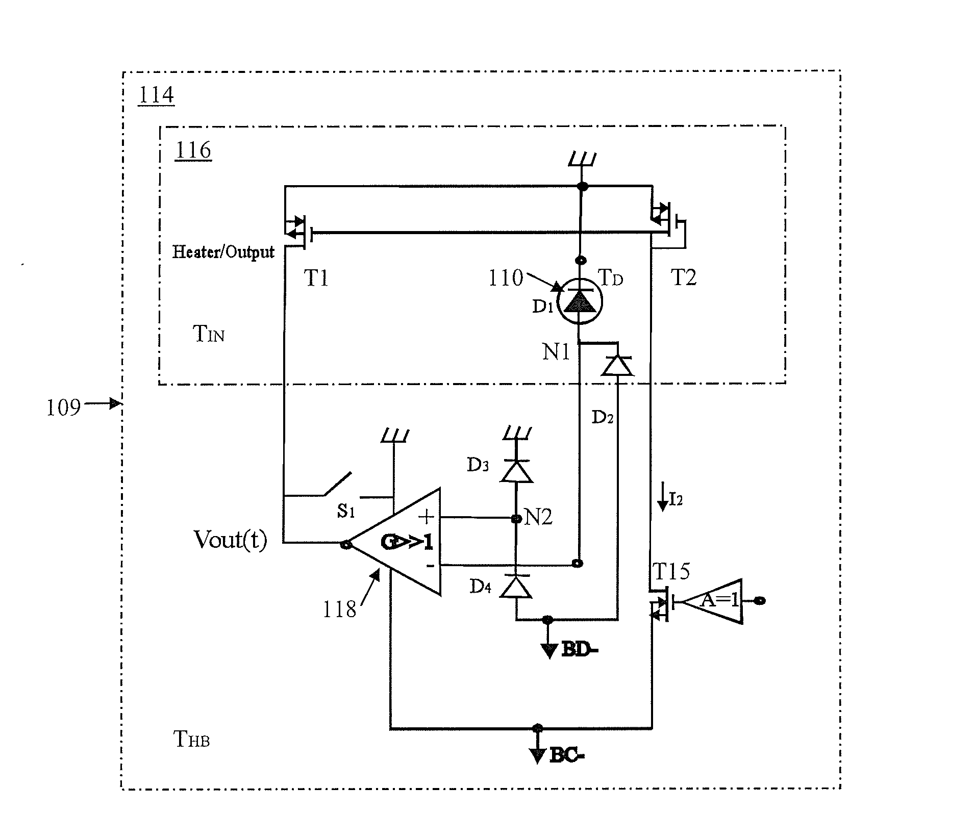
[0092]A diagram of a bolometer pixel 109 with an electro-thermal feedback circuit according to an embodiment of the present invention is shown in FIG. 7. A plurality of such pixels can be arranged in an array, such as in rows and columns, to create nil array of pixels to form a focal plane with bolometer pixels. Each bolometer pixel 109 includes a detector stage 110, an intermediate stage 116, and a heat bath stage 114. Within each pixel, the detector, intermediate and heat bath stages are connected in spaced relation to on another by a low thermal conductance bridge structure, e.g., as described in U.S. Pat. No. 7,361,900 entitled “‘I’ Beam Bridge Interconnection for Ultra-Sensitive Silicon Sensor,” U.S. Pat. No. 7,064,328 entitled “Ultra Sensitive Silicon Sensor Millimeter Wave Passive Imager” or U.S. Pat. No. 6,489,615 entitled “Ultra Sensitive Silicon Sensor,” the disclosures of which are incorporated herein by reference. It will be appreciated that the bolometer pixel can be fa...


PUM


Abstract

Electro-thermal feedback is utilized for reducing the effective thermal conductance between the detector stage of a bolometer pixel in a thermal radiation sensor assembly and the environment through its mechanical support structure and electrical interconnects, thereby coming closer to achieving thermal conductance limited primarily through photon radiation. Minimization of the effective thermal conductance associated with the mechanical support structure and electrical interconnects is achieved by electro-thermal feedback that adjusts the temperature of an intermediate stage and the mechanical support structure and electrical interconnects, connecting it to the detector stage, to equal the temperature of the bolometer pixel's detector stage (i.e., by active thermal isolation). Increased temperature sensitivity is preferably achieved through temperature sensing with reverse biased Schottky diodes connected in series.

Description

GOVERNMENT RIGHTS NOTICE[0001]This invention was made with government support under U.S. Government Contract No. W911 QX-04-C0117. The Government has certain rights to this invention.BACKGROUND OF THE INVENTION[0002]1. Technical Field[0003]This invention relates generally to ultra sensitive silicon sensors (USSS), and more particularly to an electro-thermal feedback circuit providing active thermal isolation using a series temperature-sensing diode configuration.[0004]2. Description of the Background Art[0005]Bolometers are used in many imaging applications because they provide spectral versatility. Bolometers are most commonly used in low cost and reduced sensitivity long-wavelength infrared (LWIR) cameras. Bolometers have also been used, at cryogenic temperatures, for microwave imaging. Bolometers inherently respond over a broad band and this makes them viable for imaging in different spectral bands.[0006]Quantum detectors, operating above liquid Helium temperatures, offer better ...

Claims


Application Information

Patent Timeline
IPC IPC(8): H01L27/144H01L31/09
CPCG01J5/061G01J5/20H01L27/14649H01L27/14603G01J5/24
Inventor BLUZER, NATHAN
Owner NORTHROP GRUMMAN SYST CORP
Why Eureka
Try Eureka