Anti-reflection film and infrared optical element

Active Publication Date: 2011-10-06
FUJIFILM CORP
View PDF4 Cites 16 Cited by
  • Summary
  • Abstract
  • Description
  • Claims
  • Application Information

AI Technical Summary

Benefits of technology

[0021]The infrared optical element may further include a weather resistant layer formed on the second thin film layer to improve a weather resistance property of the anti-reflection film.
[0022]According to the present invention, it is possible to inexpensively provide an infrared anti-reflection film that

Problems solved by technology

The infrared transmitting glass described above, however, is expensive and has a cost disadvantage.
Furthermore, since the infrared transmitting glass described above has a crystalline structure, a processing method thereof is limited to polishing.
This results in difficulty in processing into a complex configuration such as a microlens array.
Thus, it is known that just processing of the infrared transmitting glass into a desired outside shape of the lens or the like is not enough to obtain incident light intensity sufficient for imaging.
Furthermore, use of an expensive crystalline base made of the germanium or the like causes cost increase, in the optical element of the infrared camera.
However, if a conventional anti-reflection film designed for the germanium crystalline base is provided on a surface of the chalcogenide glass base, adhesion of the anti-reflection film is impaired.
Also, the anti-reflection film designed for the germanium crystalline base often contains a layer made of an expensive material such as germanium.
Thus, provision of the anti-reflection film that is designed for the germanium crystalline b

Method used


Image

  • Anti-reflection film and infrared optical element
  • Anti-reflection film and infrared optical element
  • Anti-reflection film and infrared optical element

Examples


Embodiment Construction

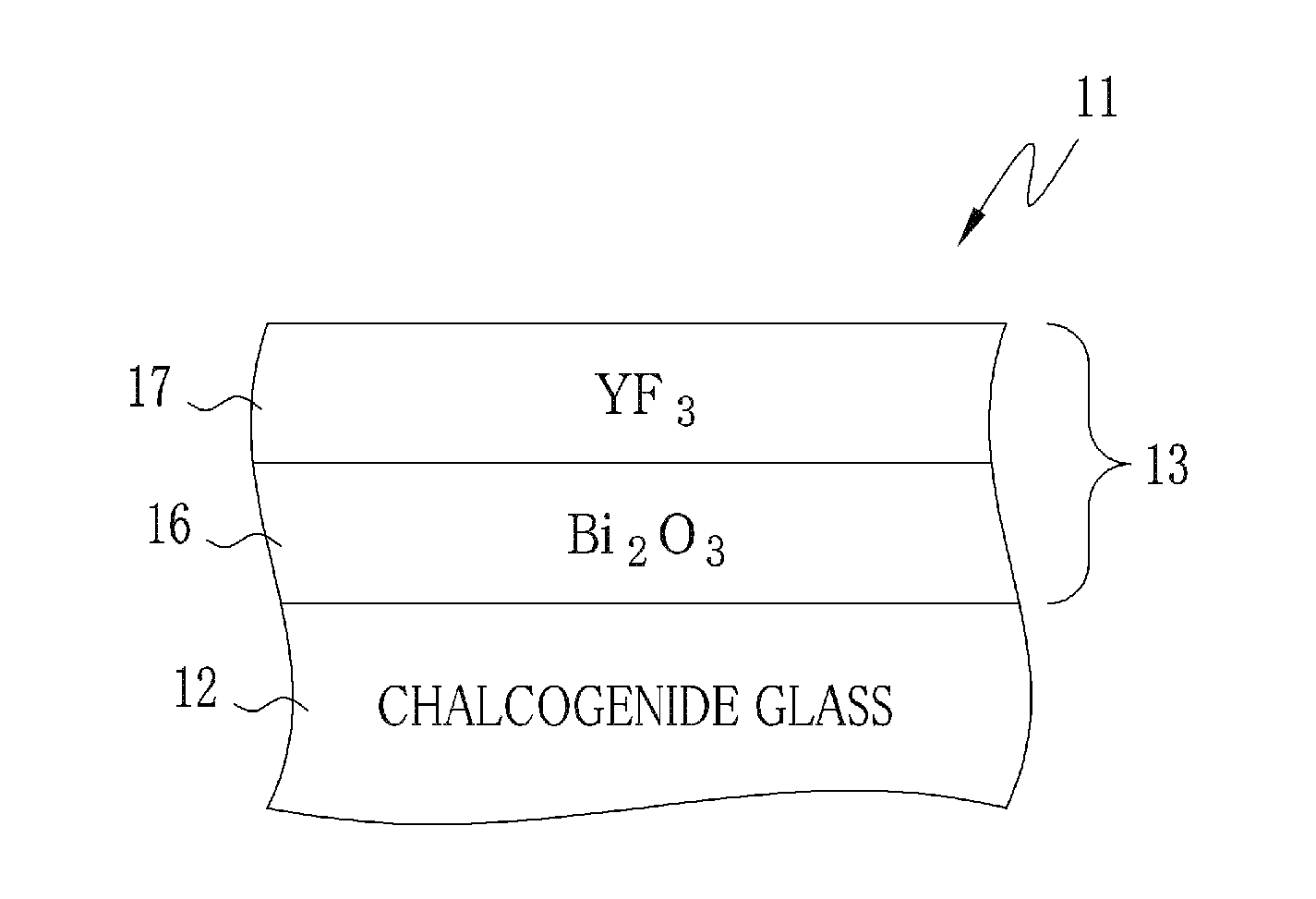
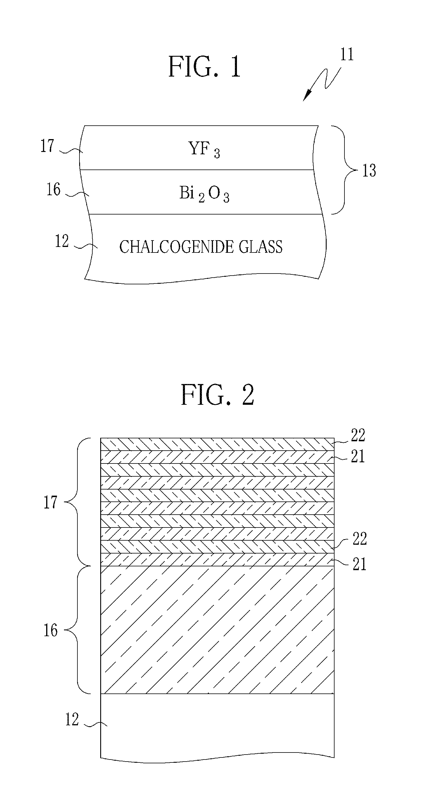
[0030]Referring to FIG. 1, a lens 11 is used in imaging of far-infrared radiation having wavelengths of 3.0 to 1000 μm. The lens 11 is constituted of a base 12 and an anti-reflection film 13 provided on a surface of the base 12. The base 12 is flat in FIG. 1, but is spherical in actual fact. Note that, when an optical element is a prism or filter, the base 12 has a plate shape.

[0031]The base 12 is made of chalcogenide glass, which has a high refractivity of approximately 2.6 in a wavelength band (3.0 to 1000 μm) described above, and has sulfur, selenium, or tellurium (so-called chalcogens) as main ingredients. The chalcogenide glass is inexpensive and superior in processability into a shape of the optical element such as a lens, as compared with other infrared transmitting glass for making a germanium crystalline base and the like. In description below, the base 12 is made of the chalcogenide glass molded into a shape of the lens 11, and the surface of the base 12 is smoothly finish...


PUM

PropertyMeasurementUnit
Thicknessaaaaaaaaaa
Thicknessaaaaaaaaaa
Electrical resistanceaaaaaaaaaa

Abstract

An anti-reflection film provided on a surface of a chalcogenide glass base includes a first thin film layer and a second thin film layer. The first thin film layer is composed of a single layer of Bi2O3 formed by ion beam assisted deposition. The second thin film layer made of YF3 includes assisted layers and non-assisted layers laminated alternately. The assisted layers are formed by the ion beam assisted deposition, while the non-assisted layers are formed without assistance of an ion beam. The assisted layer is superior in adhesion and surface flatness or smoothness. On the other hand, the non-assisted layer has small internal stress. The second thin film layer functions as a buffer to relieve the internal stress of the first and second thin film layers.

Description

BACKGROUND OF THE INVENTION[0001]1. Field of the Invention[0002]The present invention relates to an infrared optical element and an anti-reflection film used therein.[0003]2. Description Related to the Prior Art[0004]An infrared camera that captures an image using infrared radiation is widely available in recent years. As is widely known, the infrared camera is suitable for imaging in a dark place or through a screen i.e. a thin sheet of cloth. On account of this characteristic, the infrared camera is often set up in various facilities such as a store and a shop as a security or surveillance camera for crime or disaster prevention. The infrared camera is also used in measurement of water volume of a dam, measurement of traffic, and the like. Furthermore, a safe driving support system using the infrared camera is recently known. In this system, the infrared camera is provided on a car body, and a live image captured by the infrared camera is displayed on a monitor installed in a car....

Claims


Application Information

Patent Timeline
IPC IPC(8): B32B17/06G02B1/11C23C14/06G02B1/115
CPCB32B2551/00C03C17/3452Y10T428/265G02B1/115C03C2217/734B32B17/06C03C17/06G02B1/11
Inventor KURIHARA, TADAYUKI
Owner FUJIFILM CORP
Why Eureka
Try Eureka