Surface and gas phase doping of iii-v semiconductors

a technology of surface and gas phase doping and semiconductors, which is applied in the direction of semiconductor devices, basic electric elements, electrical apparatus, etc., can solve the problems of compound semiconductors, stoichiometry can be altered, and the control of post-growth dopant profiles of iii-v compound semiconductors has not been well addressed

Active Publication Date: 2012-01-26
RGT UNIV OF CALIFORNIA
View PDF5 Cites 19 Cited by
  • Summary
  • Abstract
  • Description
  • Claims
  • Application Information

AI Technical Summary

Benefits of technology

[0007]The invention provides III-V semiconductor devices and methods of doping III-V semiconductors. Embodiments of the invention provide post-deposition (or post-growth) doping of compound semiconductors. In acco

Problems solved by technology

However, since the device processing requirements are significantly different from elemental semiconductors such as silicon (Si), III-V compound semiconductors impose a major challenge on nanoscale III-V device fabrication.
Among the many challenges, controlling the post-growth dopant profiles in III-V compound semiconductors deterministically has not been well addressed.
This process, however, presents problems for compound semiconductors, which consist of two or more chemically and electronically nonequivalent lattice sites.
Specifically, the stoichiometry can be altered and difficult to recover from implantation induced crystal damage.
The residual damage can lead to higher junction leakage and lowe

Method used


Image

  • Surface and gas phase doping of iii-v semiconductors
  • Surface and gas phase doping of iii-v semiconductors
  • Surface and gas phase doping of iii-v semiconductors

Examples


example 1

S-MLD to Form N-Doped InAs

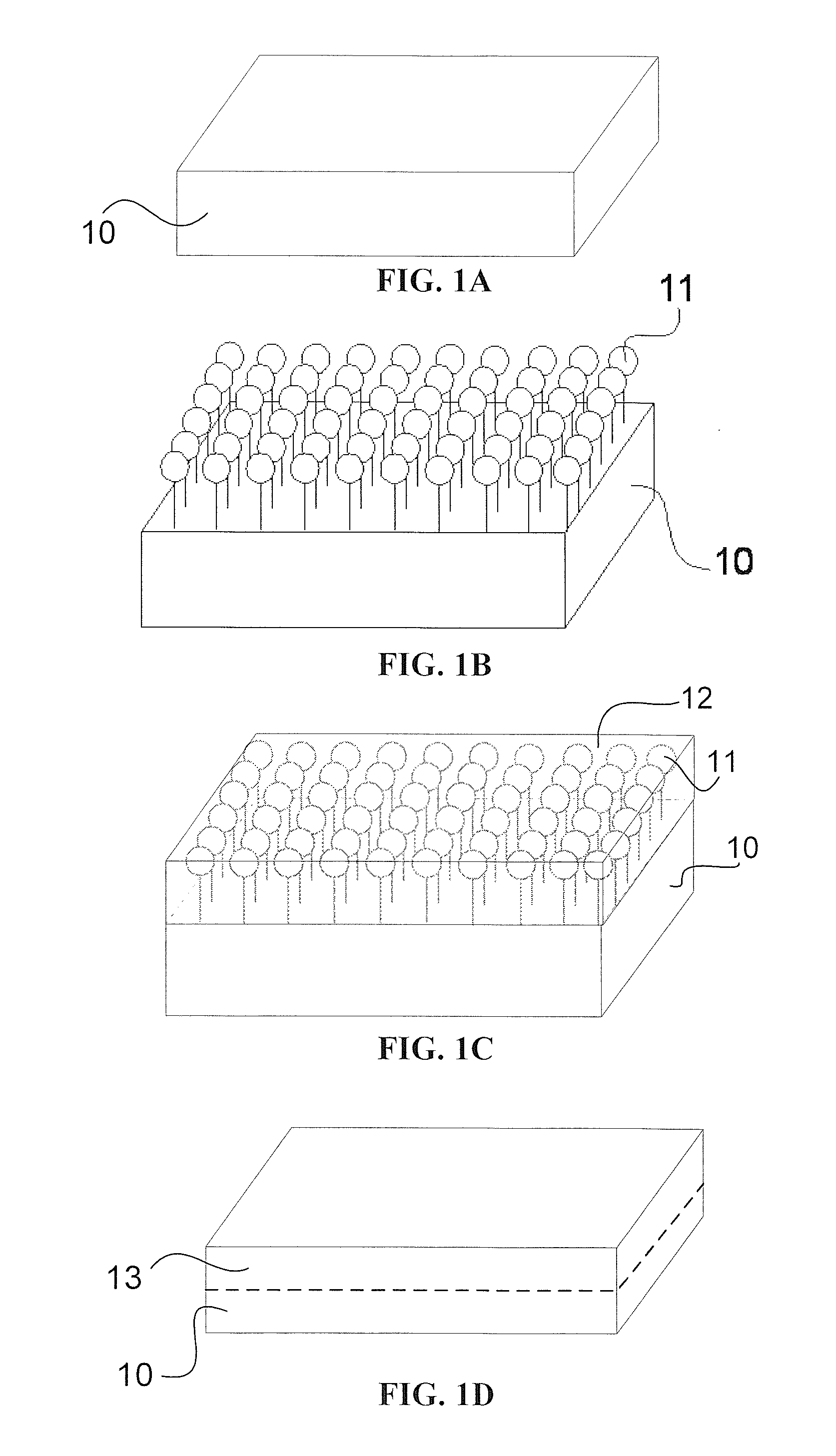
[0053]To dope InAs substrates, InAs (001) substrates can be placed in an ammonium sulfide ((NH4)2SX) solution with excess sulfur. For the experiments, the (NH4)2S, solution is 20% in water, Sigma Aldrich, and the excess sulfur is 0.2 g S per 15 ml of solution. The (NH4)2S, solution is maintained in a water bath at 35° C. The InAs (001) substrates can be initially cleaned with acetone and isopropanol in preparation of the S-MLD process.

[0054]To allow S monolayer formation on the substrate surface, the reaction is performed for 15 min. The InAs substrates are then rinsed in de-ionized water and immediately capped with an oxide. The capping oxide can be electronbeam evaporated silicon oxide (SiO2). Subsequently, thermal annealing is performed to drive in the S atoms to the desired junction depth. For the experiments, the thermal annealing was performed from 350° C. to 450° C. for 300 s.

[0055]FIG. 5 provides a characterization of the S monolayer formation. The ...

example 2

n+ / p+ Tunnel Diodes Through S-MLD of Heavily Zn-Doped InAs Substrates

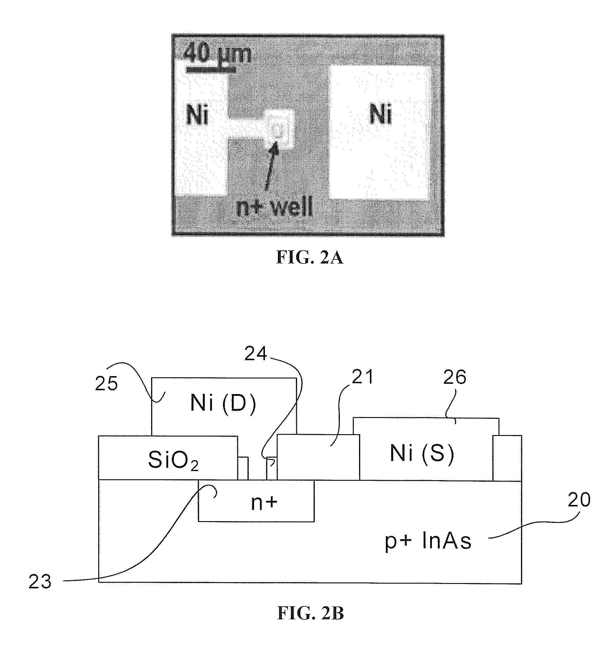
[0058]The MLD technique of embodiments of the subject invention can be applied to form devices having doped regions. To examine the electrical properties of the S monolayer doped junctions of embodiments of the invention, n+ / p+ tunnel diodes were fabricated on heavily Zn-doped InAs substrates (NB˜6×1018 cm−3).

[0059]FIGS. 2A and 2B show a plan view optical image and a cross-sectional view schematic, respectively, of a representative diode formed by a sulfur monolayer doping (S-MLD) of a p+ InAs substrate.

[0060]For the experiment example, referring to FIGS. 2A and 2B, 125 nm of field oxide 21 was deposited on the heavily Zn-doped InAs substrate 20 by electron-beam evaporation. Photolithography and wet etching using 50:1 hydrofluoric acid was used to define the well regions 23. The sulfur-containing monolayer was then assembled on the exposed InAs well regions following the technique described in Example 1, and a 35 n...

example 3

InAs NW Fabrication

[0067]InAs NWs used for experiment example embodiments were grown using the vapor-liquid-solid (VLS) method by chemical vapor deposition in a two-zone tube furnace using solid InAs powder source. A 0.5 nm thick Ni film was annealed at 800° C. for 10 min to create nanoparticles that serve as catalysts. A substrate temperature of 490° C., source temperature of 720° C., pressure of 5 torr with H2 carrier gas (200 SCCM flow rate) were used. The grown NWs were harvested by sonication in anhydrous ethanol and dropcasted on Si substrates.


PUM


Abstract

Compound semiconductor devices and methods of doping compound semiconductors are provided. Embodiments of the invention provide post-deposition (or post-growth) doping of compound semiconductors, enabling nanoscale compound semiconductor devices including diodes and transistors. In one method, a self-limiting monolayer technique with an annealing step is used to form shallow junctions. By forming a sulfur monolayer on a surface of an InAs substrate and performing a thermal annealing to drive the sulfur into the InAs substrate, n-type doping for InAs-based devices can be achieved. The monolayer can be formed by surface chemistry reactions or a gas phase deposition of the dopant. In another method, a gas-phase technique with surface diffusion is used to form doped regions. By performing gas-phase surface diffusion of Zn into InAs, p-type doping for InAs-based devices can be achieved. Both bulk and nanowire devices using compound semiconductors can be fabricated using these surface and gas-phase doping processes.

Description

[0001]This invention was made with government support under Contract No. HR0011-07-3-0002 awarded by DARPA and Grant No. 0826145 awarded by the National Science Foundation. The U.S. Government has rights in this invention.BACKGROUND OF THE INVENTION[0002]As transistor dimensions continue to shrink in order to increase density and performance, existing device structures and materials are reaching the threshold for many desirable device characteristics. To this end, new materials for existing device structures and novel transistor structures are being explored.[0003]In recent years, III-V compound semiconductors, such as indium arsenide (InAs), gallium arsenide (GaAs), and their alloy indium gallium arsenide (InGaAs), have become materials of interest for the future active channel materials of metal-oxide-semiconductor field-effect transistors (MOSFETs) and as materials for transistors with nanowire (NW) channels.[0004]III-V compound semiconductors are drawing interest because of thei...

Claims


Application Information

Patent Timeline
IPC IPC(8): H01L29/12H01L21/22H01L29/06
CPCH01L21/2233H01L21/228H01L29/78681H01L29/068H01L29/207H01L29/0673
Inventor JAVEY, ALIFORD, ALEXANDRA C.HO, JOHNNY C.
Owner RGT UNIV OF CALIFORNIA
Why Eureka
Try Eureka