Grid for radiation imaging and method for producing the same

Inactive Publication Date: 2012-12-06
FUJIFILM CORP
View PDF3 Cites 16 Cited by
  • Summary
  • Abstract
  • Description
  • Claims
  • Application Information

AI Technical Summary

Benefits of technology

[0058]The grid may be bent, so it is easy to form the grid of a converging structure.
[0059]According to the grid for the radiation imaging of the present invention, bridging portions are provided to couple the radiation transmitting sections. Thereby, the strength of the grid is increased.
[0060]The semiconductor is used for the radiation transmitting sections and the substrate to be bonded to the grid layer. Thereby, diffusion of the radiation absorbing material such as Au or the like is prevented. Thus, the reduction of the grid performance due to the diffusion of the radiation absorbing material is prevented.
[0061]The depression portions are provided between the grid layer and the support layer that supports the grid layer. A contact area between the grid layer and the support layer reduces. Thereby, loads applied to the bonding surfaces during the bonding increase. Thus, high bonding strength is obtained. The anchor layer for supporting t

Problems solved by technology

This method is susceptible to the influence of the photosensitive polymer in processing accuracy, so the grid cannot be produced with high accuracy.
Because polymer is soft, grid patterns such as plate-like patterns standing upright on a substrate are likely to be deformed by sticking (a phenomenon in which adjacent patterns stick to each other) caused by swinging or vibration of a solution during the development or surface tension of water during drying.
Thus, it is difficult to maintain the uniformity in width and height of the grid with high accuracy.
This significantly degrades the performance of the grid.
In addition, there are few domestic facilities capable of performing synchrotron radiatio

Method used


Image

  • Grid for radiation imaging and method for producing the same
  • Grid for radiation imaging and method for producing the same
  • Grid for radiation imaging and method for producing the same

Examples


first embodiment

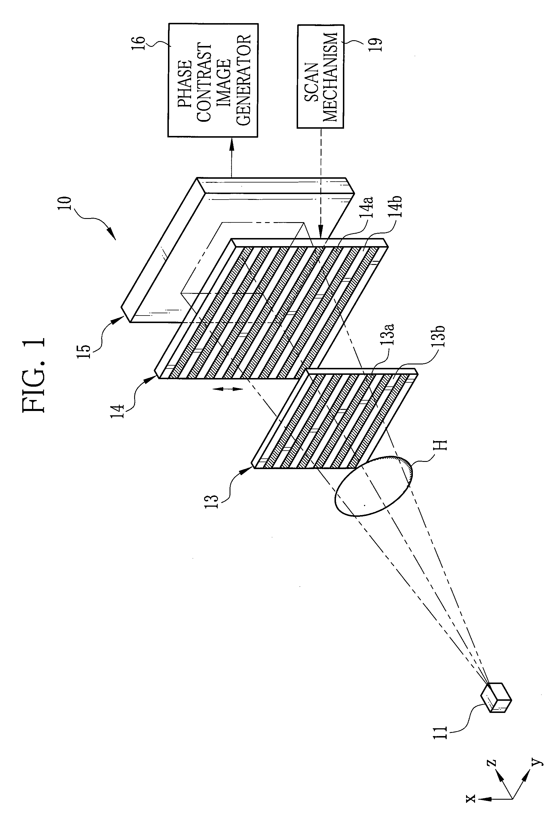
[0146]FIG. 1 is a conceptual view showing an X-ray imaging system 10 of a first embodiment. The X-ray imaging system 10 is provided with an X-ray source 11, a first grid 13, a second grid 14, and an X-ray image detector 15. The X-ray source 11 has, for example, a rotating-anode type X-ray tube and a collimator for restricting an X-ray emission field. The X-ray source 11 emits X-ray to an object H. The first grid 13 and the second grid 14 are absorption grids. The first and second grids 13 and 14 are arranged to oppose the X-ray source 11 in a z direction that is a direction of X-ray emission.

[0147]The X-ray source 11 and the first grid 13 are spaced apart enough to place the object H. A distance between the first and second grids 13 and 14 is equal to or less than a minimum Talbot length. The X-ray imaging system 10 of this embodiment does not use the Talbot effect. Instead, the X-ray imaging system 10 projects the X-ray to take a phase contrast image.

[0148]The X-ray image detector ...

second embodiment

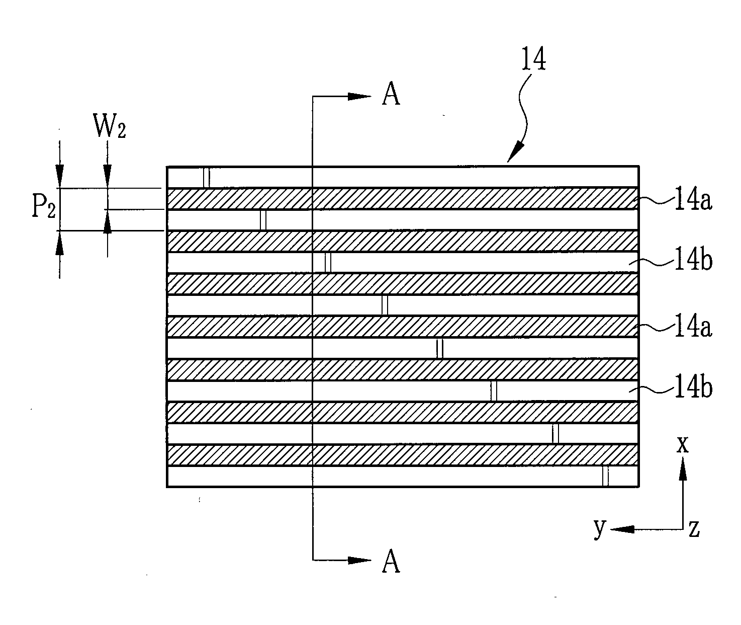
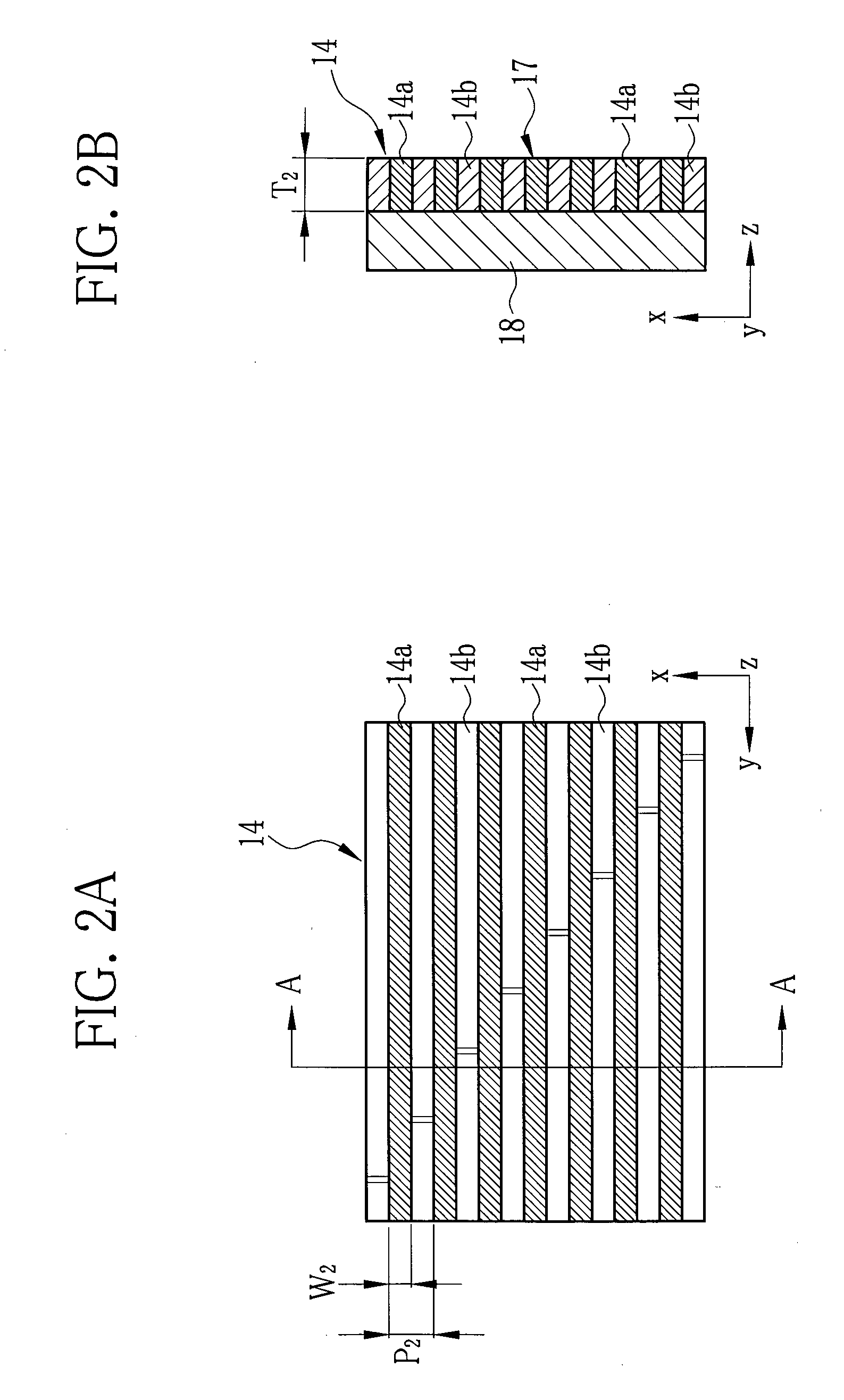
[0172]In the first embodiment, the conductive substrate 18 made of a metal plate is used as the support layer for the grid layer 17 and as the seed layer for electroplating. Alternatively, a substrate composed of a plurality of layers may be used as the conductive substrate 18. FIG. 4A is a plan view showing a second grid 30 of this embodiment viewed from the X-ray image detector 15 side. FIG. 4B is a cross-section taken along a line A-A in FIG. 4A.

[0173]The second grid 30 is composed of the grid layer 17, a conductive thin-layer 31, and a support substrate 32. The grid layer 17 is composed of a plurality of the X-ray absorbing sections 14a and a plurality of the X-ray transmitting sections 14b. Each of the conductive thin-layer 31 and the support substrate 32 has X-ray transmission properties which do not interfere with the grid performance of the grid layer 17. The conductive thin-layer 31 is used as the seed layer for the electroplating during the production of the second grid 30...

third embodiment

[0180]In the above embodiments, the grooves 20a are filled with the Au 27 by the electroplating method. Due to the in-plane distribution of the Au in the grooves 20a, however, the grooves 20a may be filled unevenly with the Au 27. To solve this problem, in this embodiment, as shown in a step of FIG. 6G performed after the step of FIG. 5F, the electroplating is performed such that the Au overflows the grooves 20a to cover the entire top face of the etching substrate 20. After the electroplating, as shown in FIG. 6H, the top face of the etching substrate 20 is polished. Thereby, the Au 27 and the etch mask 25 extending out of the grooves 20a are removed.

[0181]In the dry etching using the Bosch process, periodical recesses called scallops appear noticeably on the top face, which increase variations in width dimensions of the grooves 20a. Polishing the top face of the etching substrate 20 eliminates the scallops. The thickness of the etching substrate 20 to be polished to eliminate the ...


PUM

PropertyMeasurementUnit
Thicknessaaaaaaaaaa
Electrical resistivityaaaaaaaaaa
Thicknessaaaaaaaaaa

Abstract

A conductive substrate (18) and an etching substrate (20) are bonded to each other. An etch mask (25) is formed on the etching substrate (20) using a photolithography technique. On the etching substrate (20), grooves (20a) and X-ray transmitting sections (14b) are formed by dry etching using Bosch process. The grooves (20a) are filled with Au (27) by an electroplating method using the conductive substrate (18) as an electrode. Thus, X-ray absorbing sections (14a) are formed.

Description

TECHNICAL FIELD[0001]The present invention relates to a grid for radiation imaging and a method for producing the same.BACKGROUND ART[0002]It is known that X-ray changes its intensity and phase by interaction between the X-ray and an object when the X-ray is incident on the object. The phase of the X-ray interacts with the object more strongly than the intensity of the X-ray does. Researches have been conducted actively on X-ray phase imaging that uses the above property of the X-ray to get a high contrast image (hereinafter referred to as phase contrast image) of an object with low X-ray absorption properties based on the phase change (angular change) of the X-ray caused by the object.[0003]An X-ray imaging system using the Talbot effect caused by two transmission-type diffraction gratings (grids) is devised as one type of X-ray phase imaging (for example, Japanese Patent No. 4608679 and C. David et al., “Differential X-ray phase contrast imaging using a shearing interferometer”, A...

Claims


Application Information

Patent Timeline
IPC IPC(8): G21K1/06B29D11/00G01N23/04
CPCA61B6/484G21K1/025G21K1/06G21K2201/06C25D3/00A61B6/4092A61B6/4291G21K2207/005G21K2201/067G21K1/02
Inventor KANEKO, YASUHISA
Owner FUJIFILM CORP
Why Eureka
Try Eureka