
Chemically amplified positive resist composition and patterning process

a positive resist and composition technology, applied in the field of chemically amplified positive resist composition and patterning process, can solve the problems of system, crack resistance during cracking, pattern deformation, and difficult to increase the integration density of bumps, etc., to achieve short development time, high sensitivity, and high degree of removal

Active Publication Date: 2013-01-31
SHIN ETSU CHEM IND CO LTD
View PDF6 Cites 18 Cited by
  • Summary
  • Abstract
  • Description
  • Claims
  • Application Information

AI Technical Summary

Benefits of technology

The invention is a special resist material that can be applied to a surface to create patterns. It has unique properties that make it sensitive to certain chemicals and can be easily removed. The resist material is also strong enough to resist damage during plating processes. Overall, this invention provides a reliable and efficient way to create detailed patterns on metal surfaces.

Problems solved by technology

While bumps of mushroom shape are formed using conventional thin film resist, such bump shape is difficult to increase the integration density by increasing the number of pins on LSI or reducing the pin spacing.
Both the compositions are improved in crack resistance, but have a possibility that the pattern profile is degraded owing to the reduced contrast of resist film.
This system, however, is insufficient with respect to crack resistance during or after the plating step in the gold plating application.
This implies that the resist material adapted for solder bump pattern formation may have problems with respect to sensitivity and resist pattern profile.
While positive resist compositions comprising a novolac resin and a naphthoquinonediazide-containing compound are commonly used in the art, as described in JP-B S46-16049 and JP-A 2004-198915, thick films thereof having a thickness of several tens of μm to about 100 μm are degraded in sensitivity, which reduces the productivity efficiency of pattern formation, causes the pattern profile to be tapered, and leads to profile deficiency against the requirement to shape bumps with vertical sidewalls (or straight sidewalls).
In connection with the chemically amplified resist composition used as the solder bump-forming resist material requiring a film thickness of several tens of μm to about 100 μm, when polyhydroxystyrene in which some phenolic hydroxyl groups are substituted with acetal groups as acid labile group is used as the base resin (JP-A 2002-006503), a problem arises that a long time is necessary for development because of the thick film.
The long development time leads to drawbacks such as a time-consuming process and low production efficiency.
When the pattern of chemically amplified positive resist composition is immersed in the strong acid based solder plating bath, the strong acid system exposes the pattern to very rigorous conditions, giving rise to the problems that not only cracks generate as mentioned previously, but also the pattern swells and deforms.
Although the chemically amplified positive resist composition is preferred as the solder bump-forming resist material, many problems remain unsolved including a long development time, and film swell and pattern deformation upon immersion in plating bath.
Now that the solder bump-forming resist composition is formed into a thick film, if a compound resulting from acid elimination has a boiling point of up to 20° C. under atmospheric pressure, it can gasify, remain within the film, and form large bubbles in the film, adversely affecting the pattern profile.
However, the chemically amplified positive resist composition comprising a resin having a tertiary alkyl ester as acid labile group may fail to gain a high resolution in the lithography process of forming a resist pattern because the acid elimination reaction of the acid labile group is inferior to that of acetal groups.
For this reason, the resist material film which is to become alkali soluble after exposure and development is extremely reduced in alkali solubility, failing to gain a high resolution.
In this way, the acid generation function can be lost.
The footing profile can be transferred to solder bumps near the substrate as cutouts, with a possibility that the pattern collapses.

Method used


Image

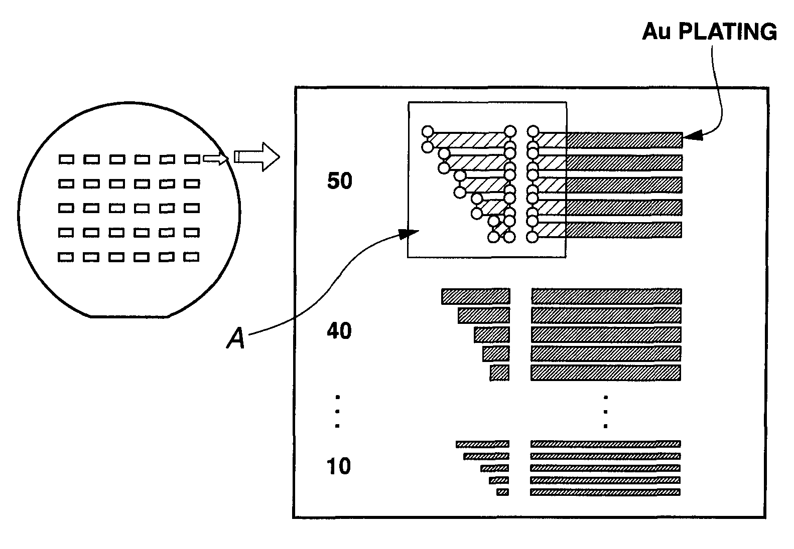
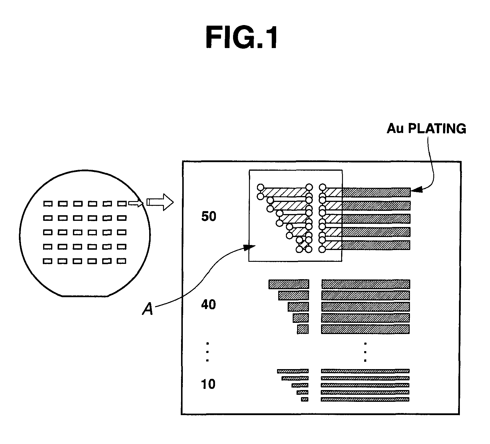
  • Chemically amplified positive resist composition and patterning process
  • Chemically amplified positive resist composition and patterning process
  • Chemically amplified positive resist composition and patterning process

Examples


example

[0154]Examples of the invention are given below by way of illustration and not by way of limitation.

examples 1 to 18

[0155]A resist solution was prepared by selecting two polymers (Polymers 1 to 6 having recurring units identified below) as base resin, an acid generator (PAG-1 or PAG-2), a basic compound (Amine 1), a benzotriazole compound (B-1 to B-4), a dissolution inhibitor (D-1), and a surfactant in accordance with the formulation shown in Table 1, dissolving them in propylene glycol monomethyl ether acetate (PGMEA), and filtering through a membrane filter having a pore size of 1.0 μm. The resist solution was spin coated onto a substrate (which was a 6-inch silicon wafer having copper deposited thereon by sputtering), and soft baked on a hot plate under the conditions shown in Table 2 to form a resist film having a thickness of 50.0 μm. It is noted that the film thickness was measured by a spectrometric film thickness measurement system Lambda Ace VM1200 by Dainippon Screen Mfg. Co., Ltd.


PUM

PropertyMeasurementUnit
wavelengthaaaaaaaaaa
thicknessaaaaaaaaaa
thickaaaaaaaaaa

Abstract

A chemically amplified positive resist composition is provided comprising an alkali-insoluble or substantially alkali-insoluble polymer having an acid labile group-protected acidic functional group, an alkyl vinyl ether polymer, a photoacid generator, and a benzotriazole compound in a solvent. The composition forms on a substrate a resist film of 5-100 μm thick which can be briefly developed to form a pattern at a high sensitivity and a high degree of removal or dissolution to bottom.

Description

CROSS-REFERENCE TO RELATED APPLICATION[0001]This non-provisional application claims priority under 35 U.S.C. §119(a) on Patent Application No. 2011-161860 filed in Japan on Jul. 25, 2011, the entire contents of which are hereby incorporated by reference.TECHNICAL FIELD[0002]This invention relates to a chemically amplified positive resist composition which can be patterned by exposure to UV radiation having a wavelength of up to 500 nm (near and deep-UV regions), e.g., i- and g-lines, and a pattern forming process.[0003]The resist composition is coated onto a substrate to form a relatively thick resist film of 5 to 100 μm thick which is exposed and developed to form a pattern. The composition has an improved sensitivity and allows for effective removal or dissolution near the substrate or at the pattern bottom. The development time can be reduced although a long time is otherwise required for the development of a thick resist film. While a chemically amplified positive resist composi...

Claims


Application Information

Patent Timeline
Patent Type & Authority Applications(United States)
IPC IPC(8): G03F7/027C25D5/02G03F7/20
CPCG03F7/0392Y10S430/11G03F7/40G03F7/0397G03F7/039G03F7/26
Inventor YASUDA, HIROYUKITAKEMURA, KATSUYA
Owner SHIN ETSU CHEM IND CO LTD
Learn More