Carbon nanotube crossbar based nano-architecture

a crossbar and nano-architecture technology, applied in nanoinformatics, instruments, electric pulse generator details, etc., can solve the problems of significant process variation, inability to avoid variations by manufacturing process improvement, and significant challenges to overcome before reliable high-performance nano-electronic circuits can be achieved

Active Publication Date: 2013-02-07
BOARD OF RGT THE UNIV OF TEXAS SYST
View PDF7 Cites 9 Cited by
  • Summary
  • Abstract
  • Description
  • Claims
  • Application Information

AI Technical Summary

Benefits of technology

[0030]In one embodiment, a double gate carbon nanotube field effect transistor (RDG-CNFET), which is reconfigurable to be open, short, FET, or via, includes a first carbon nanotube (CNT) as the front gate, which is either metallic or doped to p- or n-type; a second CNT as the source, the drain, and the channel, which is orthogonal to the first CNT, and doped to p-n-p, p-i-p, n-p-n, or n-i-n type, where i stands for intrinsic (un-doped), the source and the drain are doped to n- or p-type opposite to that of the channel (if the channel is doped); a third CNT as the back gate, which has the same orientation as the first CNT, and is either metallic or doped to p- or n-type; an electrically bistable molecules which are coated around the front gate and sandwiched between the front gate and the source / drain regions, and dielectric and redox active molecules coated around the back gate and sandwiched between the back gate and the source / drain regions.

Problems solved by technology

However, significant challenges need to be overcome before reliable high performance nanoelectronic circuits can be achieved.
As minimum layout feature size is becoming smaller than lithography light wavelength, traditional lithography based manufacturing process can no longer achieve the needed resolution, leading to significant process variation.
Such variations cannot be avoided by manufacturing process improvement, and is inherent at nanometer scale, as is dictated by the stochastic nature of quantum physics.
Nanoscale devices have achieved high performance in the absence of significant load, however, system performance bottleneck lies in global interconnects.
However, no nanoelectronic architecture has been proposed which is solely based on carbon nanotubes and carbon nanotube field effect transistors.
The reasons include lack of a self-assembly process which could form complex carbon nanotube structures, or, absence of a reconfigurable carbon nanotube device which could provide functionality and reliability.
Another outstanding challenge for realizing such nanoelectronic systems is how to precisely address an individual nanoscale wire (e.g., carbon nanotube) in an array.
Designing a nano-addressing circuit is a challenging task, because (1) the nanoscale layout cannot be manufactured precisely unless it is of a regular structure, and (2) the nano-addressing circuit cannot be based on reconfigurability since it provides reconfigurability to the rest of the nanoelectronic system.
Existing nano-addressing circuits require precise layout control such as lithography, doping, or etching, which is highly unlike to achieve alignment at the nanometer scale due to the presence of prevalent defects and significant process variations.
These techniques also exhibit certain levels of randomness, which brings nanoscale wires that cannot be differentiated or addressed, and requires testing schemes which associate nanoscale wires with addresses.
However, large resistance exists at CNT-metal contacts, reducing the performance advantage of CNTs over copper interconnects.
This device has the most mature manufacturing technique up to today, while two problems limit its future: (a) The metal-nanotube contact severely limits current.
(b) The ambipolar conduction means this device cannot be applied to conventional circuit design methods.(2) A MOSFET-like CNFET is made by doping a continuous nanotube on both sides of the gate, thus forming the source / drain regions.
It was observed that passive device (diode / resistor) based circuits lack signal gain to recover from signal attenuation, while combining with CMOS circuits compromises scaling advantages.
Latches based on negative differential resistors (NDRs) were proposed, which, unfortunately, have become obsolete since the publication.
Such architectures achieve compromised scaling advantage in term of device density.
However, the optimal size of a combinational logic block is typically small (e.g., of 30-50 gates), which results in significant CMOS circuitry overhead in such architectures.
However, such precise layout design is unlikely to achieve at a sublithographic nanometer scale (without significantly compromised yield), because nanoscale structures are expected to be bottom-up self-assembled regular structures, instead of defined by a top-down process like lithography.
As a result, these existing nano-addressing structures have limited yield, e.g., there is certain probability that two nanoscale wires have identical or similar gate configuration due to process variation.
Furthermore, nanoscale wires are mostly partially selected, e.g., they may not achieve the ideal conductivity upon selected, due to process variations such as misalignment, dopant variation, etc.

Method used


Image

  • Carbon nanotube crossbar based nano-architecture
  • Carbon nanotube crossbar based nano-architecture
  • Carbon nanotube crossbar based nano-architecture

Examples


Embodiment Construction

[0043]It is to be understood the present invention is not limited to particular devices or systems, which may, of course, vary. It is also to be understood that the terminology used herein is for the purpose of describing particular embodiments only, and is not intended to be limiting. As used in this specification and the appended claims, the singular forms “a”, “an”, and “the” include singular and plural referents unless the content clearly dictates otherwise.

Reconfigurable Double Gate-Carbon Nanotube Field Effect Transistor

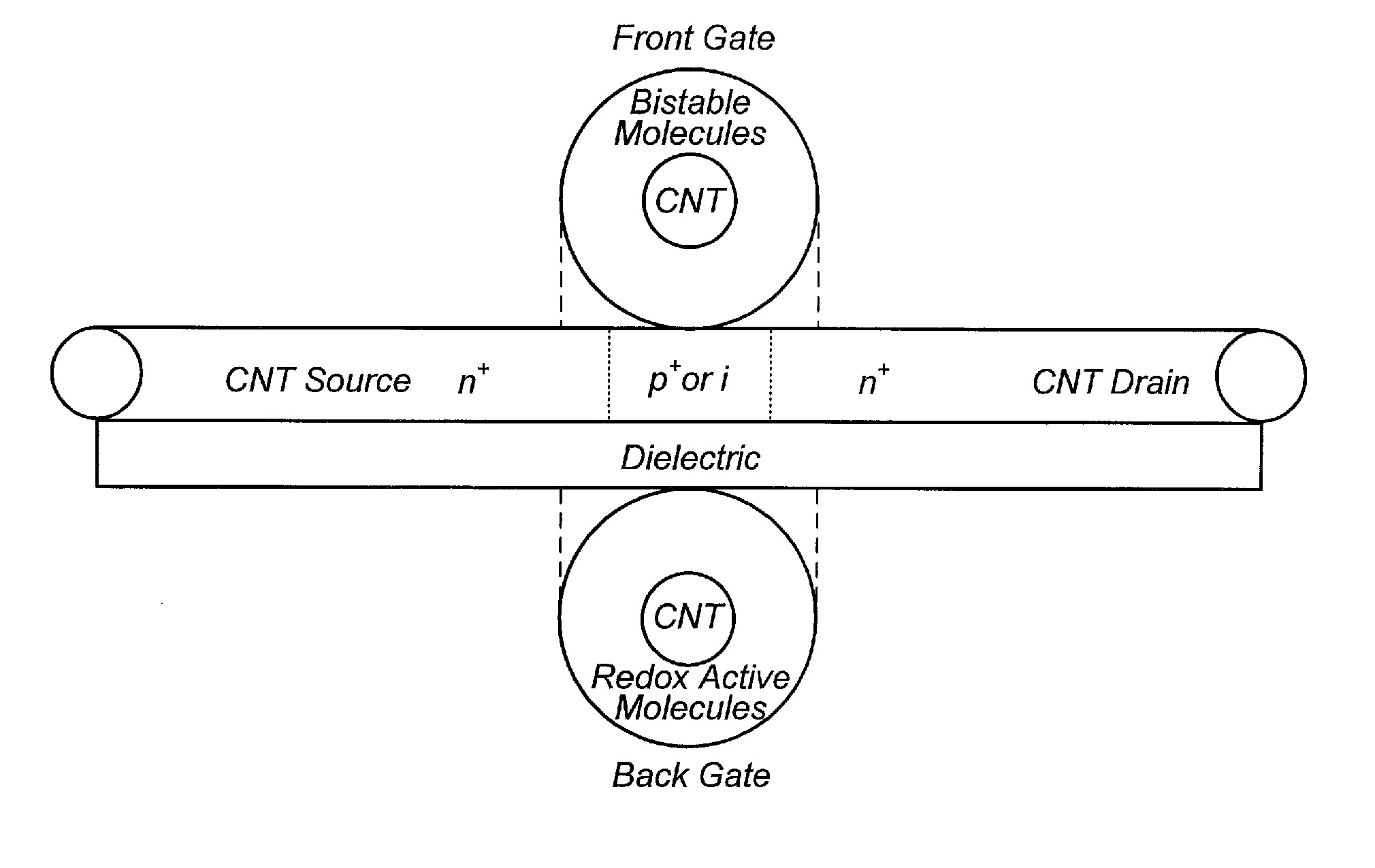
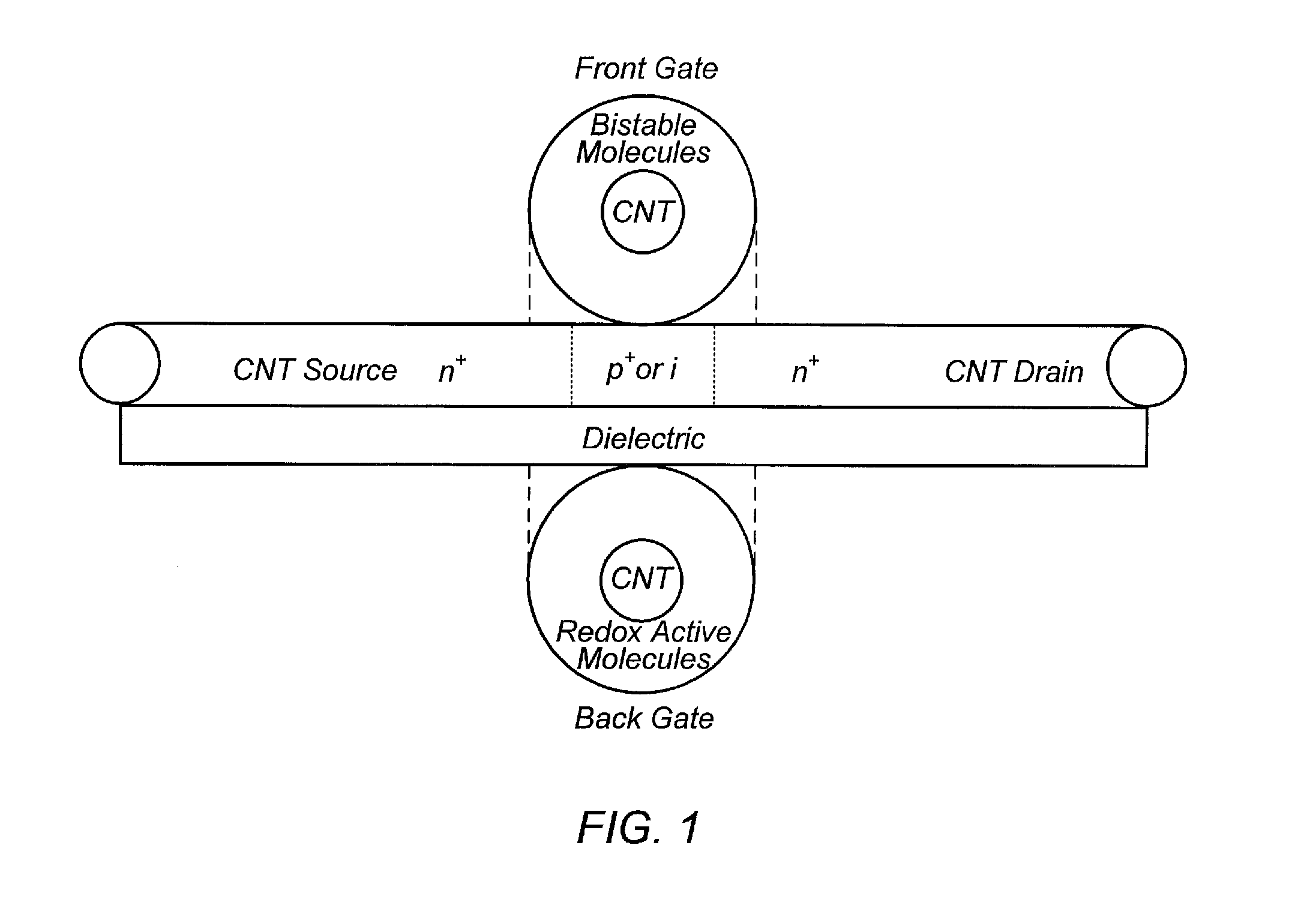
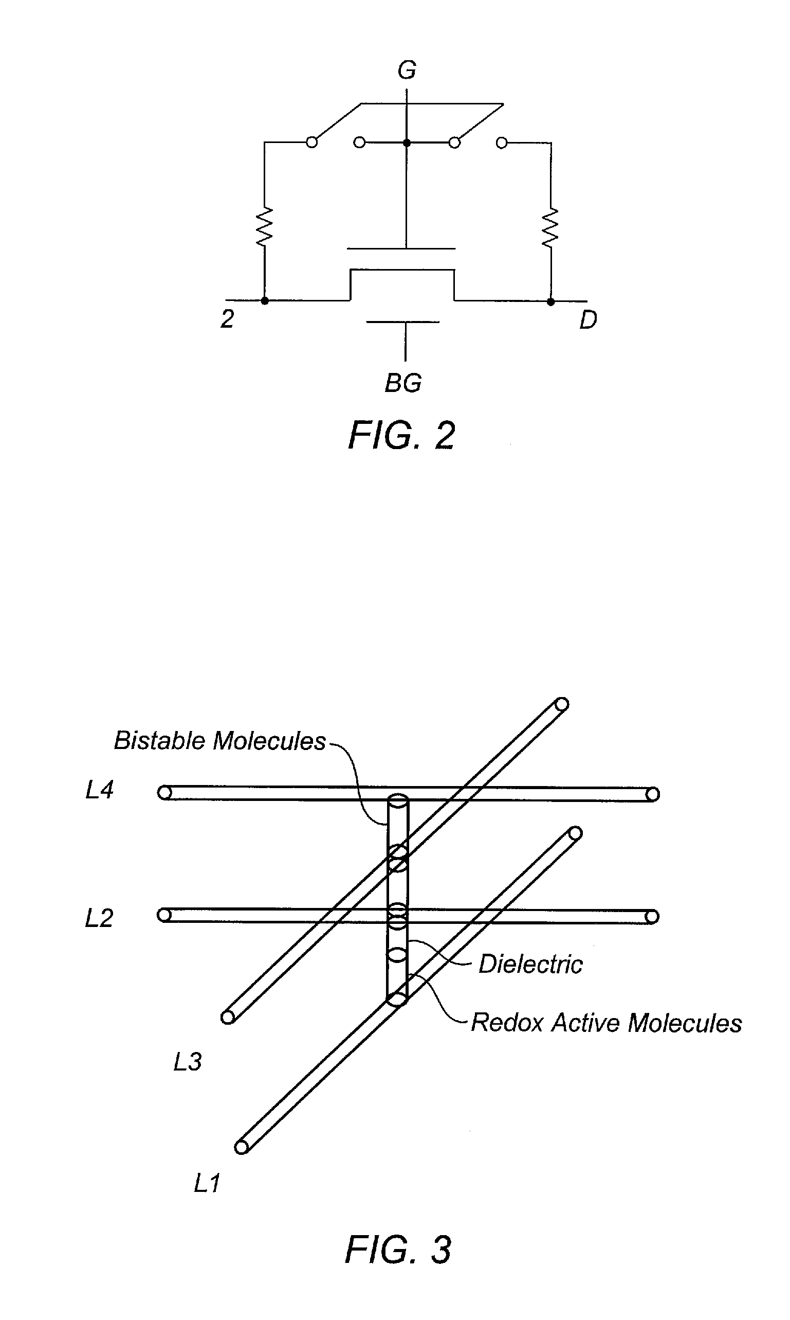
[0044]FIG. 1 is an illustration of the proposed reconfigurable double gate CNFET device, which is constructed by sandwiching electrically bistable molecules in a double gate CNFET. The double gate CNFET is constructed by three overlapping orthogonal carbon nanotubes. The top and the bottom carbon nanotubes form the front gate and the back gate, while doping the carbon nanotube in the middle layer forms the source and the drain of a n- or p-type MOSFET-like CNFE...


PUM

PropertyMeasurementUnit
channel lengthaaaaaaaaaa
gate widthaaaaaaaaaa
resistanceaaaaaaaaaa

Abstract

Carbon nanotubes (CNTs) and carbon nanotube field effect transistors (CNFETs) have demonstrated extraordinary properties and are widely accepted as the building blocks of next generation VLSI circuits. A CNT crossbar based nano-architecture, includes layers of orthogonal carbon nanotubes with electrically bistable and charge holding molecules at each crossing, forming a dense array of reconfigurable double gate carbon nanotube field effect transistors (RDG-CNFETs) and programmable interconnects, which is addressed via a voltage controlled nanotube addressing circuits on the boundaries.

Description

BACKGROUND OF THE INVENTION[0001]1. Field of the Invention[0002]The invention generally relates to nanoelectronic devices. More particularly, the invention relates to nanoelectronic devices that include carbon nanotubes.[0003]2. Description of the Relevant Art[0004]Silicon based CMOS technology scaling has driven the semiconductor industry towards cost minimization and performance improvement in the past four decades, and is rapidly approaching its end. On the other hand, nanotechnology has achieved significant progress in recent years, fabricating a variety of nanometer scale devices, e.g., molecular diodes and carbon nanotube field effect transistors. This has provided new opportunities for VLSI circuits to achieve continuing cost minimization and performance improvement in a post-silicon-based-CMOS-technology era.[0005]However, significant challenges need to be overcome before reliable high performance nanoelectronic circuits can be achieved. Challenges that need to be overcome i...

Claims


Application Information

Patent Timeline
Patent Type & Authority Applications(United States)
IPC IPC(8): H01L29/772H03K3/01B82Y99/00
CPCB82Y10/00H01L27/283H01L27/285H01L51/102H01L51/0554H01L51/0558H01L51/0049G11C2213/14H10B20/00H10K19/202H10K19/10H10K85/225H10K85/221H10K10/482H10K10/484H10K10/82
Inventor LIU, BAO
Owner BOARD OF RGT THE UNIV OF TEXAS SYST
Why Eureka
Try Eureka