Polycrystalline cuprous oxide nanowire array production method using low-temperature electrochemical growth

a nanowire array and polycrystalline technology, applied in the direction of electroforming nanostructures, cell components, coatings, etc., can solve the problems of high temperature and high pressure conditions for manufacturing monocrystalline nanowires or nanowire arrays, complicated and expensive manufacturing processes and equipment, etc., and achieve the effect of improving the crystallinity of nanowires

Inactive Publication Date: 2013-10-17
KONKUK UNIV IND COOP CORP
View PDF3 Cites 18 Cited by
  • Summary
  • Abstract
  • Description
  • Claims
  • Application Information

AI Technical Summary

Benefits of technology

[0016]The step of manufacturing a monocrystalline copper oxide (I) nanowire array by using the nanopore alumina layer as a nanopore molding flask includes: a step of manufacturing an electrochemical deposition solution by mixing copper nitrate hydrate (Cu(NO3)2.2.5H2O) and hexamethylenetetramine; a step of stirring the electrochemical deposition solution and heating the electrochemical deposition solution in a boiling water bath; a step of stirring the electrochemical deposition solution at a predetermined temperature; a step of applying a predetermined current density to the nanopore molding flask in an electrochemical reaction solution; a step of washing an electrochemically grown nanowire with ethanol and deionized water and drying the nanowire; a step of performing a heat treatment to improve crystallinity of the nanowire; and a step of removing a nanopore membrane with an NaOH aqueous solution.

Problems solved by technology

Until the present, a technology for manufacturing monocrystalline nanowires or nanowire arrays requires high temperature and high pressure conditions or complicated and expensive manufacturing process and equipment.

Method used


Image

  • Polycrystalline cuprous oxide nanowire array production method using low-temperature electrochemical growth
  • Polycrystalline cuprous oxide nanowire array production method using low-temperature electrochemical growth
  • Polycrystalline cuprous oxide nanowire array production method using low-temperature electrochemical growth

Examples


example 1

[0027]Example 1 was a step of manufacturing a nanopore membrane (anodized alumina (AAO)) from a high-purity aluminum (Al) sheet by using a two-step anodic oxidation method.

[0028]In other words, after a high-purity aluminum sheet having a desired size was prepared, the high-purity aluminum sheet was electrolytically polished at a temperature of 10° C. for 4 minutes by applying direct current (DC) voltage of +20 V thereto in an electrolytic polishing solution (including chloric acid (HClO4) and ethanol at a volume ratio of 1:4).

[0029]Primary anodic oxidation was performed onto the electrolytically polished aluminum sheet at a temperature of 10° C. for 12 hours by applying voltage of +20 V thereto in a 0.3 M sulfuric acid (H2SO4) aqueous solution or a 0.3 M oxalic acid (H2C2O4) aqueous solution.

[0030]A porous alumina layer formed by the primary anodic oxidation was etched and removed with a mixed solution of 6 wt % of phosphoric acid (H3PO4) and 1.8 wt % of chromic acid (CrO3) at a tem...

example 2

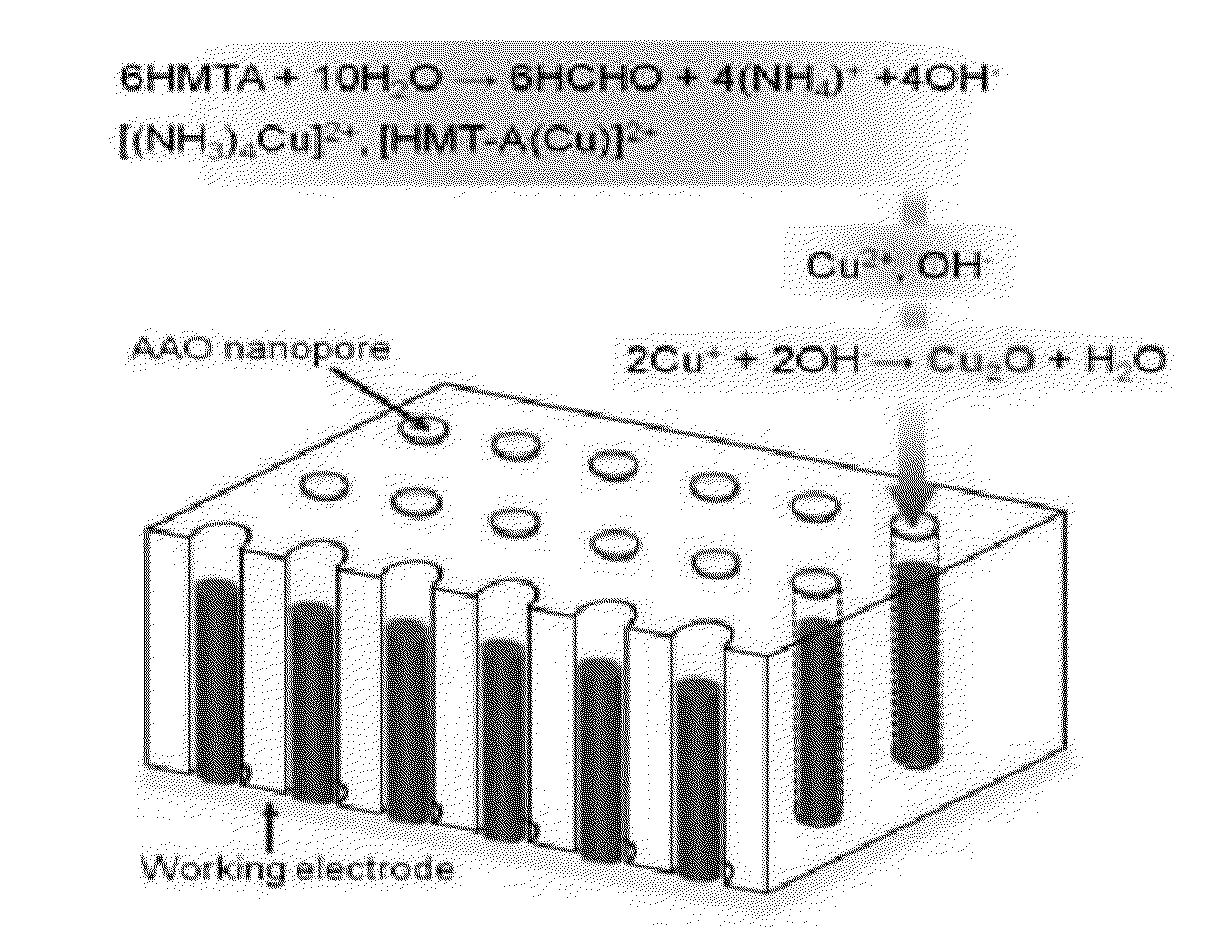
[0035]Example 2 was a step of manufacturing a monocrystalline copper oxide (I) nanowire array by using the nanopore alumina layer obtained from Example 1 as a nanopore molding flask. A 20 mM aqueous solution was prepared by mixing copper nitrate hydrate (Cu(NO3)2.2.5H2O) and hexamethylenetetramine.

[0036]Then, the prepared electrochemical deposition solution was heated in a boiling water bath until a temperature thereof reached 80° C. with stirring at a speed of 100 rpm.

[0037]Further, when the temperature of the electrochemical deposition solution reached 80° C., the electrochemical deposition solution was stirred at a speed of 100 rpm for 10 minutes.

[0038]Thereafter, a predetermined current density of 1 mA / cm2 was applied to the prepared nanopore molding flask in an electrochemical reaction solution for a desired time period.

[0039]Subsequently, an electrochemically grown nanowire was washed with ethanol and deionized water and then dried.

[0040]Then, a heat treatment was performed on...


PUM

PropertyMeasurementUnit
temperatureaaaaaaaaaa
thicknessaaaaaaaaaa

Abstract

There are provided a monocrystalline copper oxide (I) nanowire array manufacturing method using low-temperature electrochemical growth, and more particularly, to a manufacturing method allowing easy vapor deposition at low temperatures and also a monocrystalline copper oxide (I) nanowire array manufacturing method using low-temperature electrochemical growth which retains characteristics such as large-area growth, high-crystallinity nanowire, uniform radial distribution, easy length, radius adjustment, and the like.
A monocrystalline copper oxide (I) nanowire array manufacturing method of the present invention includes a step of manufacturing a nanopore alumina layer (anodized alumina (AAO)) from a high-purity aluminum (Al) sheet by using a two-step anodic oxidation method; and a step of manufacturing a monocrystalline copper oxide (I) nanowire array by using the nanopore alumina layer as a nanopore molding flask by means of a low-temperature electrochemical growth method.

Description

FIELD OF THE INVENTION[0001]The present invention relates to a monocrystalline copper oxide (I) nanowire array manufacturing method using low-temperature electrochemical growth, and more particularly, to a manufacturing method allowing easy vapor deposition at low temperatures and also a monocrystalline copper oxide (I) nanowire array manufacturing method using low-temperature electrochemical growth which retains characteristics such as large-area growth, high-crystallinity nanowire, uniform radial distribution, easy length, radius adjustment, and the like.BACKGROUND OF THE INVENTION[0002]Typically, a nanowire is a wire structure with a diameter of the order of nanometer (nm). Due to its geometrical nanostructure having a high aspect ratio and a large surface area, the nanowire is an important nano material in a wide range of future industrial fields (e.g., a semiconductor memory field, an LED field, a solar cell field, a sensor field, a catalyst field, a battery electrode material ...

Claims


Application Information

Patent Timeline
Patent Type & Authority Applications(United States)
IPC IPC(8): C25D1/04C25D11/04
CPCC25D1/04C25D11/045C25D1/006B82B3/00C23C16/06C23C16/44C25D11/04
Inventor PARK, BAE HOKANG, SUNG OONG
Owner KONKUK UNIV IND COOP CORP
Why Eureka
Try Eureka