High optical transparent two-dimensional electronic conducting system and process for generating same

a two-dimensional electronic conducting system and high optical transparency technology, applied in the field of transparent conducting materials, can solve the problems of increasing brittleness, increasing brittleness, and relatively high cost of ito, and achieve good percolation transport

Inactive Publication Date: 2014-01-16
PURDUE RES FOUND INC
View PDF1 Cites 43 Cited by
  • Summary
  • Abstract
  • Description
  • Claims
  • Application Information

AI Technical Summary

Benefits of technology

[0013]In the hybrid TCM of the invention, preferably the granular polycrystalline film and the nanowire layer separately each have a sheet resistance of 20 ohms per square or greater. The hybrid TCM has a sheet resistance below twenty ohms per square. The hybrid TCM of the invention preferably has a transmittance above ninety percent for solar radiation. Preferably the transparent electrode has a sheet resistance below twenty ohms per square and a transmittance above ninety percent for solar radiation.
[0014]In the hybrid TCM, the number of conductive nanostructures preferably is less than one half the number of grains in the granular polycrystalline film, more preferably the number of conductive nanostructures is less than one fourth the number of grains in the granular polycrystalline film.
[0015]In some embodiments, the transparent electrode may comprise a plurality of stacked layers, where each of the plurality of stacked layers comprises polycrystalline graphene that is percolation doped with metallic nanowires. The transparent electrode may have a sheet resistance below twenty ohms per square and a transmittance above ninety percent for solar radiation.
[0016]A photovoltaic cell is provided according to the invention which comprises a transparent electrode comprising polycrystalline graphene that is percolation doped with metallic nanowires, wherein the metallic nanowires do not form a percolation network for charge carriers across the transparent electrode. Because the nanowires by themselves have poor electrical contact they do not provide good percolation transport apart from the combination with the graphene. The metallic nanowires are at sufficiently low density that they do not form a percolation network for charge carriers across the transparent electrode. The photovoltaic cell can comprise a transparent electrode comprising a plurality of stacked layers, with each of the plurality of stacked layers comprising polycrystalline graphene that is percolation doped with metallic nanowires.

Problems solved by technology

However, ITO is relatively expensive (due to limited abundance of indium), brittle, unstable, inflexible.
It increases in brittleness with aging and is chemically unstable under acid / base conditions.
Furthermore, metallic-ion diffusion from ITO into thin barrier layers may result in parasitic leakage.
These and other problems make ITO-based technologies non-ideal for applications such as thin film photovoltaics (“PVs”), flexible electronics, touch-screen displays, light emitting diodes, and the like.
However, since resistivity and transmittance are often fundamentally constrained by the intrinsic properties of a material, developing TCMs with both low sheet resistance (e.g., RS90%) has been a persistent challenge.
Approaches involving welding of the nanowires, thermal annealing under pressure, or electroplating decrease RS by improving RNW-NW, but it has been challenging to reduce overall RS below ≈30Ω / □, especially for broadband T at 90%.
However, the exfoliated approach yields samples that are too small for practical applications, and large-area synthesis approaches, including chemical vapor deposition (CVD), typically involving growth on copper foil and subsequent transfer to an arbitrary substrate, produces grain sizes typically ranging from a few micrometers to a few tens of micrometers, depending on the specific growth conditions.
These high densities of CNTs or NWs, however, reduce the transmittance of such TCMs considerably.
Moreover, even with low RS, vertical current collection in PV cells is compromised by current crowding at the small-area interface between a network of CNTs or NWs and the bulk emitter layer.
Meanwhile, experimental data suggests that there is a fundamental limitation to the sheet resistance and transmittance of pure poly-graphene films, making it difficult for poly-graphene to compete successfully with ITO.

Method used


Image

  • High optical transparent two-dimensional electronic conducting system and process for generating same
  • High optical transparent two-dimensional electronic conducting system and process for generating same
  • High optical transparent two-dimensional electronic conducting system and process for generating same

Examples


example 1

[0075]Commercial CVD SLG on copper foil (ACS Materials Co., MA) was employed. Standard procedures were followed for plasma etching of SLG from back side of Cu and layer transfer onto a 1 cm×1 cm quartz substrate (SPI Supplies, PA), including copper etching using iron nitrate solution (X. Li, et al., Science (2009), 324,1312). Commercial AgNWs (Blue Nano Inc., NC), with diameters of 70-110 nm and lengths of 20-60 μm, are dispersed in isopropyl alcohol at a concentration of 0.1 mg mL−1. AgNW networks were drop cast either after (Hybrid 1) or before (Hybrid 2) SLG transfer, with density controlled by number of drops. Finally, the hybrid films were annealed for 1 hour in forming gas at 300° C. with a 40 sccm flow rate. The schematic process flow of SLG transfer and fabrication of hybrid films is shown in FIGS. 10, 11a and 11b. SLG and Hybrid 2 films were also fabricated on transparent, flexible PET substrates (from Dupont) for mechanical bending tests.

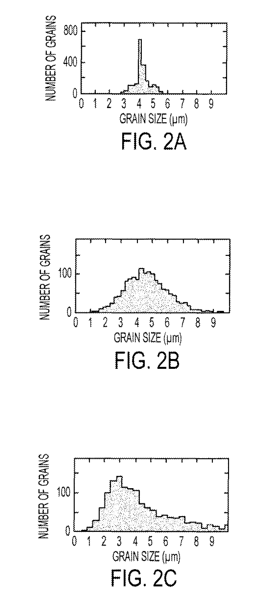
[0076]Raman spectra and Raman spati...

example 2

[0077]CTLM electrode with channel lengths of ≈7, 22, 49 and 100 μm were fabricated by evaporation of Ti / Pd / Au (thickness 1 nm / 30 nm / 20 nm) in a Kurt J. Lesker electronbeam evaporator with base pressure of ≈9×10⁻⁷ Torr, followed by lift-off. Two-terminal current vs. voltage measurements were performed using a probe station (Cascade Microtech.), Keithley 7174A switch matrix system, and a Keithley 4200 SCS semiconductor parameter analyzer. Sheet resistances were measured using CTLM, with geometry correction before sheet resistance calculation. Results can be found in Supporting Information, Figure S3 of Chen et al.

Testing and Results

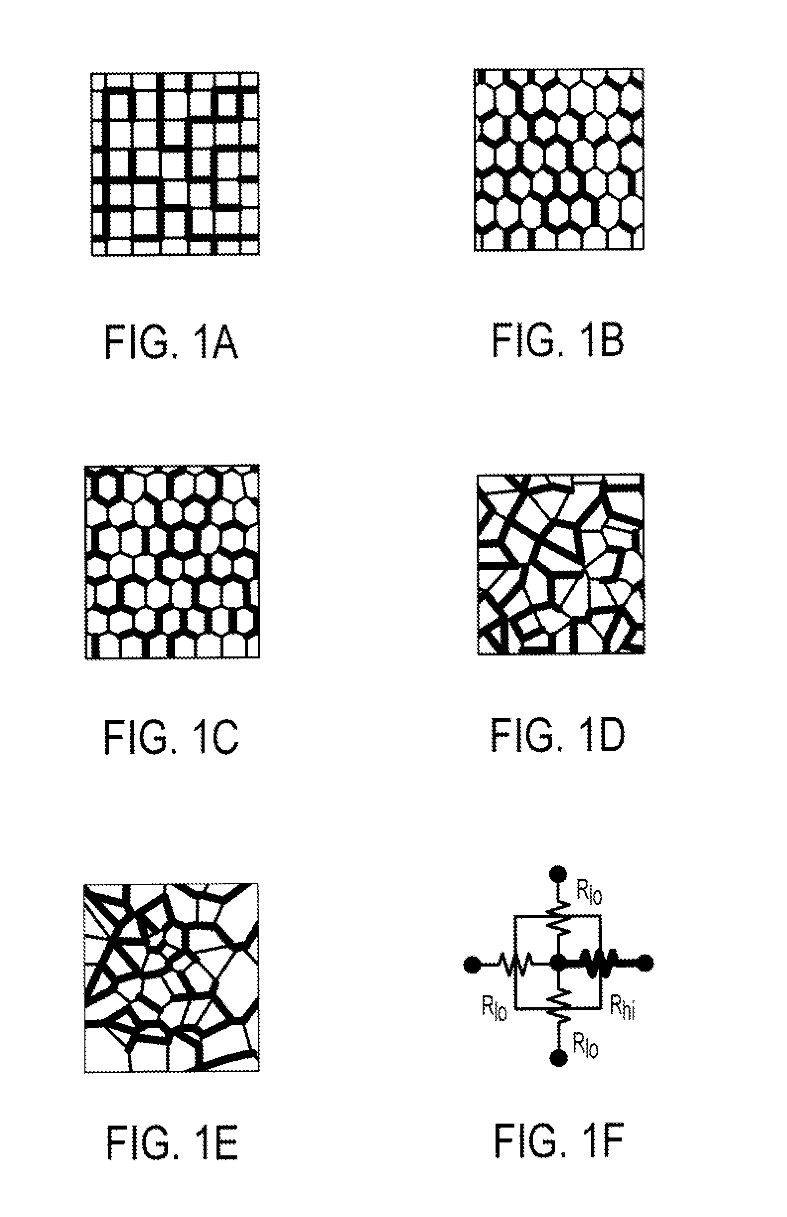
[0078]Specular and Diffusive Transmittance:

[0079]Since the surfaces of the hybrid films are textured, it is important to characterize their diffusive and specular transmittances. The diffusive spectra for the (i) quartz substrate, (ii) quartz with SLG, and (iii) the quartz with hybrid films were all measured at normal incidence using a Perkin Elmer (lambda ...


PUM

PropertyMeasurementUnit
lengthaaaaaaaaaa
sheet resistanceaaaaaaaaaa

Abstract

Hybrid transparent conducting materials are disclosed with combine a polycrystalline film and conductive nanostructures, in which the polycrystalline film is “percolation doped” with the conductive nanostructures. The polycrystalline film preferably is a single atomic layer thickness of polycrystalline graphene, and conductive nanostructures preferably are silver nanowires.

Description

[0001]This invention was made with government support under DE-SC0001085 awarded by Department of Energy. The government has certain rights in the invention.BACKGROUND OF THE INVENTION[0002]A. Field of the Invention[0003]The present disclosure relates, generally, to transparent conducting materials (“TCMs”) and, more particularly, to hybrid TCMs including a polycrystalline film that is “percolation doped” with conductive nanostructures.[0004]B. Description of the Related Art[0005]Transparent conducting electrodes (TCEs) require high transparency and low sheet resistance for applications in photovoltaics, photodetectors, flat panel displays, touch screen devices and imagers. Indium tin oxide (ITO), or other transparent conductive oxides, have typically been used, and provide a baseline sheet resistance (RS) vs. transparency (T) relationship. However, ITO is relatively expensive (due to limited abundance of indium), brittle, unstable, inflexible. It increases in brittleness with aging...

Claims


Application Information

Patent Timeline
Patent Type & Authority Applications(United States)
IPC IPC(8): G02F1/1343H01L31/0224
CPCG02F1/13439H01L31/022466G02F2202/36H01L31/1884H01B1/04B82Y10/00B82Y40/00H01L29/1606H01L29/413Y02E10/549H01L31/028Y02E10/547Y10T428/2438H01B1/02Y02P70/50H10K30/82H01L31/022491H01L31/1864
Inventor ALAM, MUHAMMAD ASHRAFULCHEN, RUIYIDAS, SUPREM R.JANES, DAVID B.JEONG, CHANGWOOK
Owner PURDUE RES FOUND INC
Why Eureka
Try Eureka