Rapid Thinning of GaN and SiC Substrates and Dry Epitaxial Lift-off

Inactive Publication Date: 2015-09-17
FARAH JOHN
View PDF6 Cites 23 Cited by
  • Summary
  • Abstract
  • Description
  • Claims
  • Application Information

AI Technical Summary

Benefits of technology

[0008]It is desired to cleave atomically flat surfaces at or very near the epi/wafer interface in order to minimize post lift-off polishing and avoid wasting substrate material. III-V materials have the advantage that devices are fabricated in epitaxially-grown layers. Thus, the epi-layer can be peeled off the substrate and transferred to a flexible carrier and the substrate can be reused to grow another epi-layer. If the quality of the surface is good and the substrate is recovered at original thickness then the substrate can be reused multiple, perhaps more than 10 times. The fragile crystalline solar cell must be supported at all times. A suitable flexible carrier is polyimide Kapton® sheet w

Problems solved by technology

Laboratories with special equipment are required to handle GaAs because it contains arsenic, which is toxic.
At $100 a piece this creates the most expensive toxic dust.
However, sola

Method used


Image

  • Rapid Thinning of GaN and SiC Substrates and Dry Epitaxial Lift-off
  • Rapid Thinning of GaN and SiC Substrates and Dry Epitaxial Lift-off
  • Rapid Thinning of GaN and SiC Substrates and Dry Epitaxial Lift-off

Examples


example 1

[0216]GaAs (110) E1eff=250 GPa, h1=370 μm, polyimide E2eff=5.8 GPa, h2=150 μm E=E1eff / E2eff=42.88, h=h1 / h2=2.467

[0217]Equations (5-9) yield:

1 / (2R)=0.3 m−1→R=1.66 m   (10)[0218]σa1=6.75 MPa[0219]σa2=16.65 MPa[0220]σb1=27.75 MPa[0221]σb2=0.26 MPa[0222]εa1=0.27×10⁻⁴ [0223]εa2=28.7×10⁻⁴ [0224]εb1=1.20×10⁻⁴ [0225]εb2=0.48×10⁻⁴

example 2

[0226]Si (111) E1eff=300 GPa, h1=200 μm, polyimide E2eff=5.8 GPa, h2=150 μm E=E1eff / E2eff=51.3, h=h1 / h2=1.333

[0227]Equations (5-9) yield:

1 / (2R)=1 m−1→R=50 cm   (11)[0228]σa1=11.4 MPa[0229]σa2=15.2 MPa[0230]σb1=59.6 MPa[0231]σb2=0.87 MPa[0232]εa1=0.38×10⁻⁴ [0233]εa2=26.2×10⁻⁴ [0234]εb1=2.0×10⁻⁴ [0235]εb2=1.5×10⁻⁴

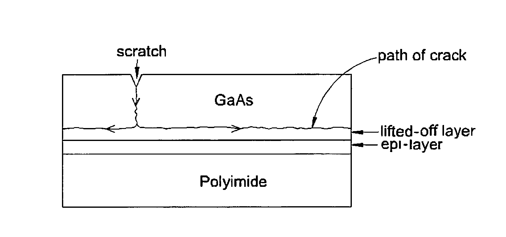
[0236]As can be seen from the two examples above, the bending stress σb1 is larger than the axial stress σa1 for both GaAs and Si, i.e. the outer half of the wafer is under tension. Thus, the stresses are not exactly as depicted in FIGS. 45 and 49, rather as shown in FIG. 52. Points B1 and C1 are almost coincident and the neutral axis is actually very close to the centroid of the GaAs cross-section. The stress in the GaAs at the polyimide / GaAs interface is compressive, which helps prevent the crack from propagating at the interface. FIG. 52 depicts the stresses due to cooling below the temperature of zero stress. In the case of heating, the stresses are reversed, i.e. the po...

example 3

[0248]Referring back to Example 1 above, GaAs (110) full thickness h1=370 μm, polyimide h2=150 μm.

Uo=(0.0328+3.467+0.193+0.0003)bL=3.693 bL   (18)

Uo=1 / 2{Fε1+Fε2+M1 / R+M2 / R}L   (14)

Equation (14) is placed directly under equation (18) in order to compare the magnitudes of the corresponding terms. The largest contributor to the elastic strain energy at full thickness by far is the axial stress in the polyimide (1 / 2Fε2). The Kapton is being stretched by 28.7×10⁻⁴, followed by bending in the GaAs, then compression in the GaAs, followed by a distant fourth, bending in the Kapton. The amount of energy that goes in bending the GaAs is 18× smaller than that goes in stretching the Kapton. The majority of the energy (93%) at full thickness is stored in the Kapton.


PUM

PropertyMeasurementUnit
Lengthaaaaaaaaaa
Fractionaaaaaaaaaa
Fractionaaaaaaaaaa

Abstract

An epitaxially grown layer III-V solar cell is separated from the growth substrate by propagating a crack close to the epi/wafer interface. The crack is driven by the elastic strain energy built up due to thermal stresses between GaAs and polyimide by cooling below room temperature. A GaAs wafer is bonded to a polyimide substrate on the epi-side and scribed on the opposite side. The crack is initiated from the scratch and guided along the interface using an epitaxially grown sacrificial layer with lower fracture toughness under the solar cell. No expensive ion implantation or lateral chemical etching of a sacrificial layer is needed. The active layer is transferred wafer-scale to inexpensive, flexible, organic substrate. The process allows re-using of the wafer to grow new cells, resulting in savings in raw materials and grinding and etching costs amounting to up to 30% of the cost of the cell. Several cells are integrated on a common blanket polyimide sheet and interconnected by copper plating. The blanket is covered with a transparent spray-on polyimide that replaces the cover glass. The solar cell is stress-balanced to remain flat on orbit.
Wide bandgap materials, such as Gallium Nitride (GaN) and Silicon Carbide (SiC) are very promising for light-emitting diodes (LEDs) and power electronics. These materials are extremely hard and difficult to machine and very expensive. The lack of good quality bulk GaN substrates with a smooth surface at a reasonable price is hampering the development of vertical devices.
A rapid thinning technique is presented by lifting-off a 20-70 μm thick layer from the surface within a fraction of a second, which leaves the surface shiny and smooth. The savings in lapping and polishing add up to 60%, when this technique is incorporated in the crystal manufacturing process. This technology also has application for backside thinning where the savings are even larger.

Description

BACKGROUND OF THE INVENTION[0001]1. Field of the Invention[0002]This invention applies to epitaxially grown solar cells and specifically to inverted solar cell structures. Inverted metamorphic III-V multi-junction solar cells achieve the highest efficiencies (>30% in space and >40% terrestrial under concentrator). These cells are grown epitaxially on Ge or GaAs wafers that are up to 700 μm thick. The solar photons are absorbed in the epitaxial layer, which is about 10 μm thick. The substrate is only for mechanical support and considered wasted from a materials point of view. Triple-junction solar cells for space cost>$250 / W. This high cost is split among the cost of the substrate (40%), epitaxial growth (30%) and front side processing including metallization (30%). Epitaxial lift-off (ELO) is used to transfer the epi-layer to a flexible substrate and reuse the Ge or GaAs wafer to grow another epi-layer. There is a need to make high efficiency solar cells thin, lightweight a...

Claims


Application Information

Patent Timeline
IPC IPC(8): B32B43/00C30B29/42C30B29/40
CPCB32B43/006B32B2457/12C30B29/42C30B29/40C30B29/36C30B29/406C30B33/06H01L21/7813Y10T156/1153Y02E10/544H01L31/06875H01L31/1892Y02P70/50H01L31/00
Inventor FARAH, JOHN
Owner FARAH JOHN
Why Eureka
Try Eureka