
Semiconductor device and electronic device including semiconductor device

a semiconductor and semiconductor technology, applied in the field of semiconductor devices, can solve problems such as deterioration of the electrical characteristics of transistors, and achieve the effects of high on-state current, high integration, and favorable electrical characteristics

Inactive Publication Date: 2015-10-08
SEMICON ENERGY LAB CO LTD
View PDF10 Cites 4 Cited by
  • Summary
  • Abstract
  • Description
  • Claims
  • Application Information

AI Technical Summary

Benefits of technology

This patent describes a semiconductor device with various desirable features such as favorable electrical characteristics, compatibility with miniaturization, high on-state current, high integration, low power consumption, reliability, and data retention. The patent also introduces a novel semiconductor device.

Problems solved by technology

Miniaturization of transistors may cause deterioration of the electrical characteristics of the transistors, such as on-state current, off-state current, threshold voltage, and a subthreshold swing (S value).

Method used


Image

  • Semiconductor device and electronic device including semiconductor device
  • Semiconductor device and electronic device including semiconductor device
  • Semiconductor device and electronic device including semiconductor device

Examples


embodiment 1

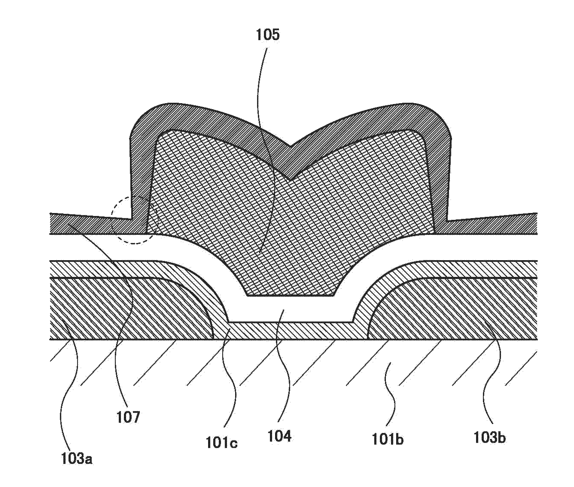
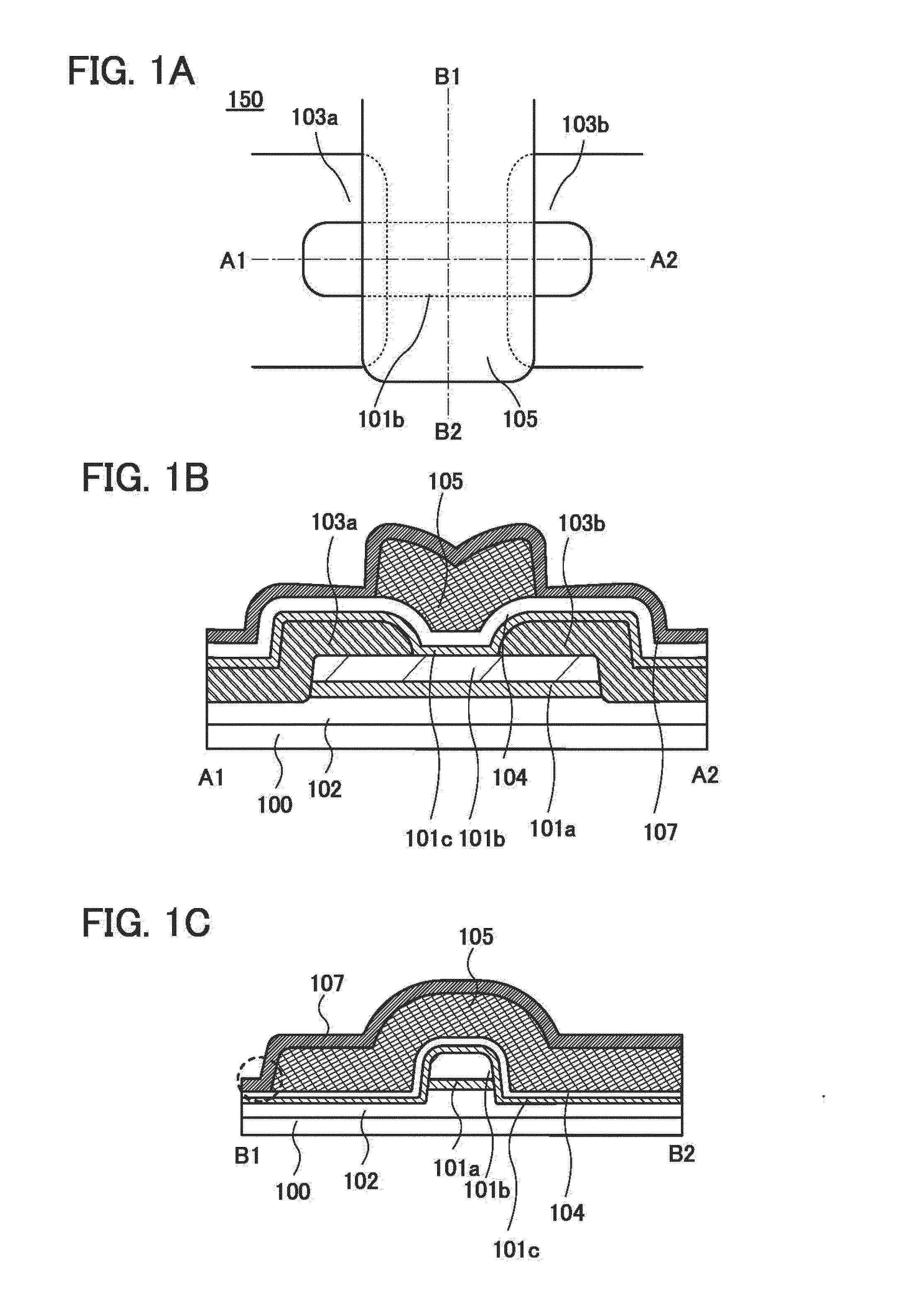
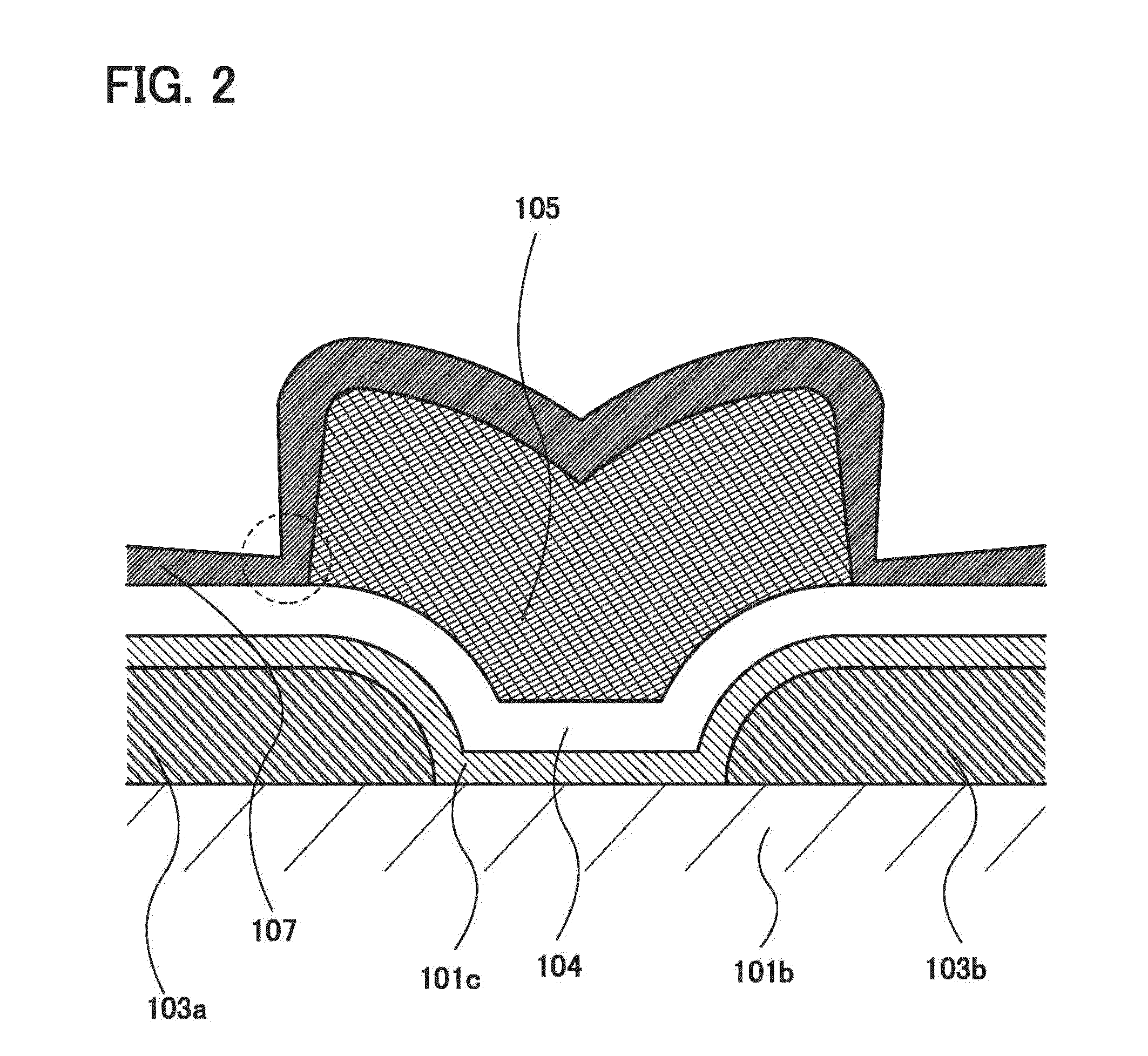
[0054]In this embodiment, a semiconductor device which is one embodiment of the present invention and a manufacturing method thereof will be described with reference to drawings. As an example of a semiconductor device, a transistor will be described.

[0055]In a transistor of one embodiment of the present invention, silicon (including strained silicon), germanium, silicon germanium, silicon carbide, gallium arsenide, aluminum gallium arsenide, indium phosphide, gallium nitride, an organic semiconductor, an oxide semiconductor, or the like can be used for a channel formation region. It is particularly preferable to use an oxide semiconductor having a wider band gap than silicon for the channel formation region.

[0056]For example, the oxide semiconductor preferably contains at least indium (In) or zinc (Zn). Further preferably, the oxide semiconductor contains an oxide represented by an In-M-Zn-based oxide (Mrepresents a metal such as Al, Ti, Ga, Ge, Y, Zr, Sn, La, Ce, or Hf).

[0057]In t...

modification example 1

[0162]Although the transistor 150 described in Embodiment 1 includes the three oxide semiconductor films, the present invention is not limited to this example. There may be a single oxide semiconductor film or two, four, or more oxide semiconductor films FIGS. 5A to 5C illustrate a case of a single oxide semiconductor film, and FIGS. 6A to 6C illustrate a case of two oxide semiconductor films.

[0163]FIGS. 5A to 5C are a top view and cross-sectional views illustrating a transistor 150a included in a semiconductor device. FIG. 5A is a top view of the transistor 150a. FIG. 5B is a cross-sectional view taken along dashed-dotted line A1-A2 in FIG. 5A. FIG. 5C is a cross-sectional view taken along dashed-dotted line B1-B2 in FIG. 5A. In FIGS. 5A to 5C, some components are enlarged, reduced in size, or omitted for easy understanding.

[0164]FIGS. 6A to 6C are a top view and cross-sectional views illustrating a transistor 150b included in a semiconductor device. FIG. 6A is a top view of the tr...

modification example 2

[0165]The above structures can each be a self-aligned structure in which the resistance of an offset region is reduced, as illustrated in FIG. 7A, FIG. 7B, or FIG. 7C.

[0166]An n-type low-resistance region 141 and an n-type low-resistance region 142 can be formed by adding an impurity using the gate electrode 105 as a mask. Examples of the method for adding the impurity include an ion implantation method, an ion doping method, and a plasma immersion ion implantation method.

[0167]An impurity such as hydrogen, helium, neon, argon, krypton, xenon, boron, nitrogen, phosphorus, or arsenic increases the conductivities of the oxide semiconductor films 101a, 101b, and 101c.

[0168]Note that a self-aligned structure illustrated in FIG. 8A may also be employed. In this structure, the n-type low-resistance regions 141 and 142 serve as source and drain regions. The low-resistance regions 141 and 142 are electrically connected to a wiring 110a and a wiring 110b with an insulating film 108 provided...


PUM


Abstract

A semiconductor device includes an oxide semiconductor film, a source electrode, a drain electrode, a gate insulating film, a gate electrode, and an insulating film. The source electrode includes a region in contact with the oxide semiconductor film. The drain electrode includes a region in contact with the oxide semiconductor film. The gate insulating film is provided between the oxide semiconductor film and the gate electrode. The insulating film is provided over the gate electrode and over the gate insulating film. The insulating film includes a first portion and a second portion. The first portion includes a step portion. The second portion includes a non-step portion. The first portion includes a portion with a first thickness. The second portion includes a portion with a second thickness. The second thickness is larger than or equal to 1.0 time and smaller than or equal to 2.0 times the first thickness.

Description

BACKGROUND OF THE INVENTION[0001]1. Field of the Invention[0002]One embodiment of the present invention relates to a semiconductor device and a manufacturing method thereof.[0003]Note that one embodiment of the present invention is not limited to the above technical field. The technical field of one embodiment of the invention disclosed in this specification and the like relates to an object, a method, or a manufacturing method. One embodiment of the present invention relates to a process, a machine, manufacture, or a composition of matter. Specifically, examples of the technical field of one embodiment of the present invention disclosed in this specification include a semiconductor device, a display device, a liquid crystal display device, a light-emitting device, a lighting device, a power storage device, a memory device, a method for driving any of them, and a method for manufacturing any of them.[0004]In this specification and the like, a semiconductor device generally means a d...

Claims


Application Information

Patent Timeline
Patent Type & Authority Applications(United States)
IPC IPC(8): H01L29/786H01L23/29H01L23/31
CPCH01L29/7869H01L23/291H01L23/3157H01L29/78606H01L29/78618H01L29/78696H01L2924/0002H01L2924/00
Inventor TANAKA, TETSUHIROSAKURADA, YUJIROOKAZAKI, YUTAKA
Owner SEMICON ENERGY LAB CO LTD
Learn More