
High efficiency broadband semiconductor nanowire devices

a broadband, semiconductor technology, applied in nanotechnology, photovoltaics, lasers, etc., can solve the problems of low requiring long tubes and limiting power output, and reducing the efficiency of such light sources

Active Publication Date: 2015-11-12
MCGILL UNIV
View PDF0 Cites 24 Cited by
  • Summary
  • Abstract
  • Description
  • Claims
  • Application Information

AI Technical Summary

Benefits of technology

The present invention provides a method for growing semiconductor structures on a substrate using nanoscale droplets of a group III element constituent of the semiconductor, which can initiate the growth of the semiconductor without the need for a foreign catalyst or other constituent elements of the semiconductor. The method includes introducing the first source of the group III element into the reaction chamber at a predetermined flow rate and pressure, and establishing operation of the reaction chamber at a predetermined set of operating conditions. The method can also include introducing both the first and second sources of the group III element into the reaction chamber at the same time, with the second source introduced at a predetermined flow rate and pressure. The semiconductor structures formed using this method can have improved properties and can be used for various applications.

Problems solved by technology

However, the efficiency of such light sources is woefully low.
However, whilst CFLs provide an immediate and visible statement by Governments and other organizations worldwide that they are addressing global climate change, environmental issues etc they are not a panacea.
Amongst the disadvantages of fluorescent lights are frequent switching limiting lifetime, health and safety from the mercury content, UV emissions which affect some materials, flicker affecting individuals with autism, epilepsy, lupus, chronic fatigue syndrome, and vertigo, radio interference, operating temperature where efficiency drops with increasing / decreasing temperature from room temperature, non-operation at below freezing, low-luminance requiring long tubes and limiting power output, dimming, and recycling through the phosphor and mercury.
As such the majority of the lighting market remains inaccessible despite the considerable research effort and investment have been expended.
This arises due to the challenges in realizing suitable LED technologies and devices using conventional quantum well structures, these including the relatively low internal quantum efficiency of these structures, the low light extraction efficiency realized, and relatively high device fabrication costs.
The extremely large inhomogeneous broadening observed makes it difficult to study the fundamental properties of InN, including the temperature dependence of the band gap and the electron concentration.
Additionally, the poorly defined wire geometry leads to uncontrolled electrical and optical properties, severely limiting their device applications.
Further the direct growth of InxGa1-xN on silicon, the most suitable substrate for InxGa1-x-N in terms of lattice and thermal mismatches, has been further complicated by the development of an amorphous SiNx layer during the initial stage of growth, see J. Grandal et al.
Attempts to adjust these growth techniques, either by the intentional introduction of hydrogen or buffer layers, such as GaN or AlN, have met with limited success.
The prior art whilst demonstrating InxGa1-xN nanowires can be grown has not yet demonstrated them with high quality and constant cross-section nor have they been grown on suitable substrates for low cost semiconductor processing.
These developments to date being hindered to a large extent by the relatively low decomposition temperature of InN (approximately 500° C.-550° C.) as well as the very high migration rate of indium.
Additionally, the prior art does not provide an effective means to control the growth and properties of InN nanowires spontaneously formed under nitrogen rich conditions.
However, increasing the efficiency of LEDs by the introduction of quantum confined structures, such as quantum wells, multi-quantum wells etc also results in a narrowing of the optical emission from the source thereby requiring that number of sources required to “blend” together for the desired white light increases, along with the cost and complexity of the devices overall.
However, whilst colloidal quantum dots are themselves efficient an optical emitter employing them can only be efficient if the colloidal quantum dots are optically pumped with an efficient emitter at the appropriate wavelength.
One of the primary causes for this low efficiency is the strain-induced polarization field in InGaN / GaN quantum wells and the resulting quantum confined Stark effect, which leads to a spatial charge separation.
As such high efficiency long wavelength (>550 nm) emission has been severely limited by the presence of large densities of misfit-dislocations related to the large lattice mismatch (approximately 11%) between InN and GaN.
However, to date such nanowire structures have reported extremely low internal quantum efficiency (<10%), due to the lack of effective carrier confinement in the wire axial direction as well as the nonradiative recombination associated with the presence of surface states.
Although progress has been made for InGaN / GaN quantum well LEDs, the performance of such devices in the green, yellow, and red wavelength ranges has been plagued by the very low efficiency, as outlined supra, and “efficiency droop”, i.e. the decrease of the external quantum efficiency with increasing current.
However, a significant roadblock for the development of nanowire LEDs is the very low quantum efficiency, and the fact that to date, there has been no report on the internal quantum efficiency of GaN-based nanowire LEDs under electrical injection.
Due to the lack of 3-dimensional carrier confinement, the radiative electron-hole recombination in commonly reported GaN nanowire LED heterostructures has been severely limited by the presence of unoccupied Ga dangling bond and / or large densities of surface defects along the nonpolar GaN surface (m-plane), which can lead to a Fermi-level pinning on the nanowire lateral surfaces.
Additionally, the device performance is adversely affected by the poor hole injection and transport processes in InGaN / GaN nanoscale heterostructures, caused by the heavy effective mass, small mobility, and low concentration of holes.
The highly non-uniform carrier distribution also lead to significantly enhanced Auger recombination and increased electron overflow, further limiting the optical emission efficiency at high injection levels
However, such phenomena have not been addressed for nanowire LEDs.
Despite the attractiveness of this approach one of the key obstacles is the availability of hydrogen.
Clearly using fossil fuel sources negates any environmental benefits of hydrogen as an energy source and even if the hydrogen economy never materializes, the production of hydrogen for industrial consumptions still consumes large amounts of energy.
Success in finding an abundant visible light active material, however, has been very limited, see for example Maeda in “Photocatalytic Water Splitting using Semiconductor Particles: History and Recent Developments” (J. Photochem. Photobiol. C: Photochem. Rev., Vol. 12, Iss. 4, pp.
However, most of these approaches cannot drive stable overall pure water splitting beyond the blue wavelength range, see for example Zoul and Maeda et al. in “Photocatalyst Releasing Hydrogen from Water” (Nature, Vol. 440, pp.
However, more recently, the use of group-III nitride semiconductors for water splitting has attracted considerable attention due to the more negative potential of the nitrogen 2p-orbital compared to that of oxygen 2p-orbital and that metal-nitrides often possess a narrow bandgap resulting in narrowband absorption.

Method used


Image

  • High efficiency broadband semiconductor nanowire devices
  • High efficiency broadband semiconductor nanowire devices
  • High efficiency broadband semiconductor nanowire devices

Examples


Embodiment Construction

[0158]The present invention is directed to semiconductor nanowire devices and more specifically to broadband optical emitters and detectors formed without foreign metal catalysis.

[0159]Reference may be made below to specific elements, numbered in accordance with the attached figures. The discussion below should be taken to be exemplary in nature, and not as limiting of the scope of the present invention. The scope of the present invention is defined in the claims, and should not be considered as limited by the implementation details described below, which as one skilled in the art will appreciate, can be modified by replacing elements with equivalent functional elements.

[0160]Nanowire Growth

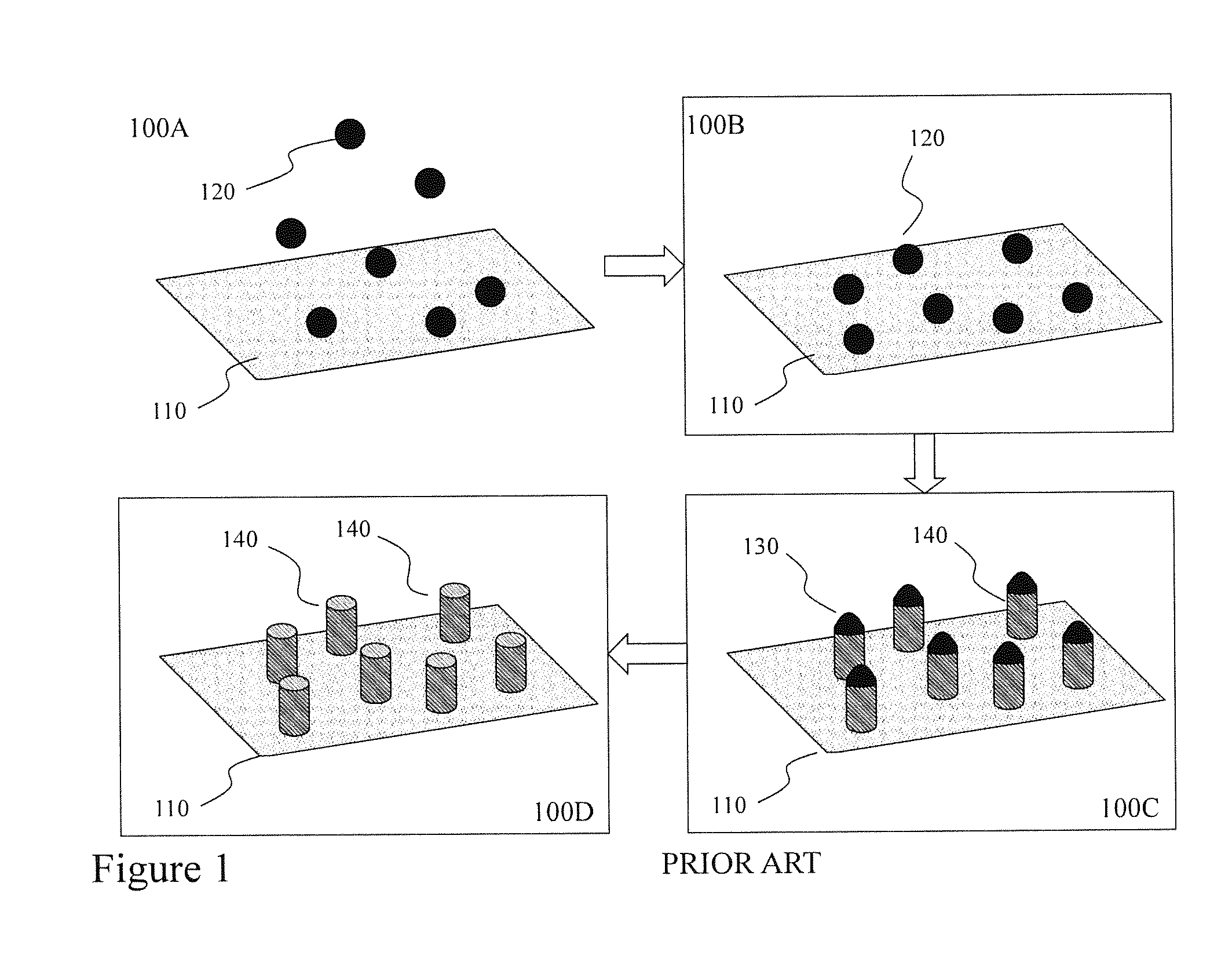
[0161]Referring to FIG. 1 there is shown a sequence of growing nanowires according to the prior art with a foreign metal catalyst. Such prior art using the vapor-liquid-solid (VLS) growth mechanism including for example J. Li et al in U.S. Pat. No. 6,831,017 entitled “Catalyst Patterning for Nano...


PUM

PropertyMeasurementUnit
quantum efficiencyaaaaaaaaaa
band gapaaaaaaaaaa
band gapaaaaaaaaaa

Abstract

Amongst the candidates for very high efficiency electronics, solid state light sources, photovoltaics, and photoelectrochemical devices, and photobiological devices are those based upon metal-nitride nanowires. Enhanced nanowire performance typically require heterostructures, quantum dots, etc which requirement that these structures are grown with relatively few defects and in a controllable reproducible manner. Additionally flexibility according to the device design requires that the nanowire at the substrate may be either InN or GaN. Methods of growing relatively defect free nanowires and associated structures for group IIIA-nitrides are presented without the requirement for foreign metal catalysts, overcoming the non-uniform growth of prior art techniques and allowing self-organizing quantum dot, quantum well and quantum dot-in-a-dot structures to be formed. Such metal-nitride nanowires and quantum structure embedded nanowires support a variety of devices including but not limited to very high efficiency electronics, solid state light sources, photovoltaics, and photoelectrochemical devices, and photobiological devices.

Description

CROSS-REFERENCE TO RELATED APPLICATIONS[0001]This patent application is being filed as a Continuation application of U.S. patent application Ser. No. 13 / 866,155 filed Apr. 19, 2013 entitled “High Efficiency Broadband Semiconductor Nanowire Devices”, currently pending.[0002]Patent application Ser. No. 13 / 866,155 claims the benefit of U.S. Provisional Patent Application 61 / 767,840 filed Feb. 22, 2013 entitled “One Step Overall Water Splitting under Visible Light using Multiband InGaN / GaN Nanowire Heterostructures.”[0003]Patent application Ser. No. 13 / 866,155 claims the benefit of U.S. Provisional Patent Application 61 / 728,310 filed Nov. 20, 2012 entitled “GaN Nanowires on Silicon Oxide.”[0004]Patent application Ser. No. 13 / 866,155 claims the benefit of U.S. Provisional Patent Application 61 / 635,965 filed Apr. 20, 2012 entitled “Photocatalytic Water Splitting Nanowire Devices and Methods of Fabricating Arrays.”[0005]Patent application Ser. No. 13 / 866,155 is a continuation-in-part of U....

Claims


Application Information

Patent Timeline
Patent Type & Authority Applications(United States)
IPC IPC(8): H01L33/06H01L33/00H01L33/14H01S5/343H01L31/0352H01S5/40H01L27/15H01L31/0735H01L31/0304H01L33/32H01L33/18
CPCH01L33/06H01L33/32H01L33/0025H01L33/14H01S5/34333H01L31/035218H01S5/4025H01L27/153H01S5/34346H01L31/0735H01L31/03044H01L33/18B82Y10/00B82Y40/00H01L21/02381H01L21/0242H01L21/02458H01L21/02505H01L21/02513H01L21/0254H01L21/02573H01L21/02603H01L21/0262H01L21/02639H01L21/02645H01L21/02664H01L29/0665H01L29/0676H01L29/068H01L29/127H01L29/20H01L29/2003H01L29/22H01L29/66469H01L29/66977H01L29/775H01L31/035227H01L31/075H01L33/005H01L2924/0002Y02E10/544Y02E10/548H01L2924/00C25B1/55H01L31/072
Inventor MI, ZETIANKIBRIA, MD GOLAM
Owner MCGILL UNIV
Learn More