Conductive paste and method for producing a semiconductor device using the same

a technology of conductive paste and semiconductor, which is applied in the direction of solid-state devices, non-conductive materials with dispersed conductive materials, basic electric elements, etc., can solve the problems of poor bonding strength of the paste, reduced glass phase which satisfactorily wets the surface of the adherend, etc., to achieve improved heat resistance and high electrical conductive properties

Active Publication Date: 2016-11-10
NAMICS CORPORATION
View PDF0 Cites 7 Cited by
  • Summary
  • Abstract
  • Description
  • Claims
  • Application Information

AI Technical Summary

Benefits of technology

[0040]The conductive paste of the present invention is advantageous in that a SiC chip and a substrate can be bonded to each other using the conductive paste by heating at a relatively low temperature (for example, at 370° C. or lower) as a heating temperature to obtain a semiconductor device. In addition, the conductive paste of the present invention is advantageous in that a semiconductor chip and a substrate can be bonded to each other using the conductive paste, and, after bonding, the bond strength between the semiconductor chip and the substrate can be maintained even in an environment at a relatively high temperature (for example, at 300 to 350° C.), and thus the obtained semiconductor device has an improved heat resistance.
[0041]Further, in the present invention, there is provided a method for producing a semiconductor device, which is advantageous in that the conductive particles contained in the conductive paste are sintered to electrically connect a semiconductor chip to a substrate, so that a semiconductor device having high electrical conductive properties can be obtained.
[0042]In the present invention, by heating the conductive paste to the remelting temperature of the glass frit contained in the conductive paste or higher and then gradually cooling the paste, it is possible to cause deposition of silver and crystals in the calcined film bonding the semiconductor chip to the substrate. The calcined film bonding the semiconductor chip to the substrate tends to have a melting temperature higher than that of the glass frit contained in the conductive paste as a raw material. In the present invention, there is provided a method for producing a semiconductor device, which is advantageous in that the obtained semiconductor device having a semiconductor chip and a substrate bonded using the conductive paste can maintain the bond strength between the substrate and the semiconductor chip even when placed in an environment at a relatively high temperature (for example, at 300 to 350° C.).

Problems solved by technology

Patent document 5 has a description showing that when the glass composition contained in the paste has a high remelting temperature, the amount of the glass phase which satisfactorily wets the surface of an adherend is reduced, so that the bond strength of the paste becomes poor.

Method used


Image

  • Conductive paste and method for producing a semiconductor device using the same
  • Conductive paste and method for producing a semiconductor device using the same
  • Conductive paste and method for producing a semiconductor device using the same

Examples


examples

[0128]The glass frit is first described below. The glass frit used in the conductive paste of the present invention is not limited by the following Examples.

[0129][Glass Frit]

[0130]Table 1 shows a glass frit substantially comprising Ag2O (B-1), V2O5 (B-2), and MoO3 (B-3), and a glass frit substantially comprising Ag2O (B-1), V2O5 (B-2), MoO3 (B-3), and ZnO (B-4). Table 2 shows a glass frit substantially comprising Ag2O (B-1), V2O5 (B-2), MoO3 (B-3), and one oxide (B-4) of TiO2, MgO, Nb2O5, BaO, Al2O3, SnO, and Fe2O3. Table 3 shows a glass frit substantially comprising Ag2O (B-1), V2O5 (B-2), MoO3 (B-3), and CuO (B-4), and a glass frit substantially comprising Ag2O (B-1), V2O5 (B-2), MoO3 (B-3), ZnO (B-4), and CuO (B-4′). In Tables 1 to 3, the values shown for components (B-1) to (B-4) are expressed in % by mass.

[0131]The method for producing the glass frit is as follows.

[0132]As raw materials for the glass frit, oxide powders shown in Tables 1 to 3 were weighed and mixed together, a...

examples 9 to 14

[0157]Conductive pastes having the respective formulations shown in Table 7 were produced, and a thermal resistance (Rth) test was performed with respect to each of the produced conductive pastes to measure an electric resistivity, evaluating the electrical conductive properties. Further, with respect to each of the conductive pastes in Examples and Comparative Examples, a die shear stress (DSS) test was performed to measure a bond strength, evaluating the heat resistance.

[0158]FIG. 3 shows scanning electron microscope (SEM) photomicrographs of the silver particles used in Examples 9 to 14, taken at magnifications of 1,000 times, 2,000 times, and 5,000 times.

example 9

Production of a Conductive Paste (MP12-102-1)

[0159]Silver particles: P318-8, K-0082P (manufactured by Metalor Technologies Corporation); The mass ratio of P318-8 silver particles and K-0082P silver particles (P318-8:K-0082) is 50:50.

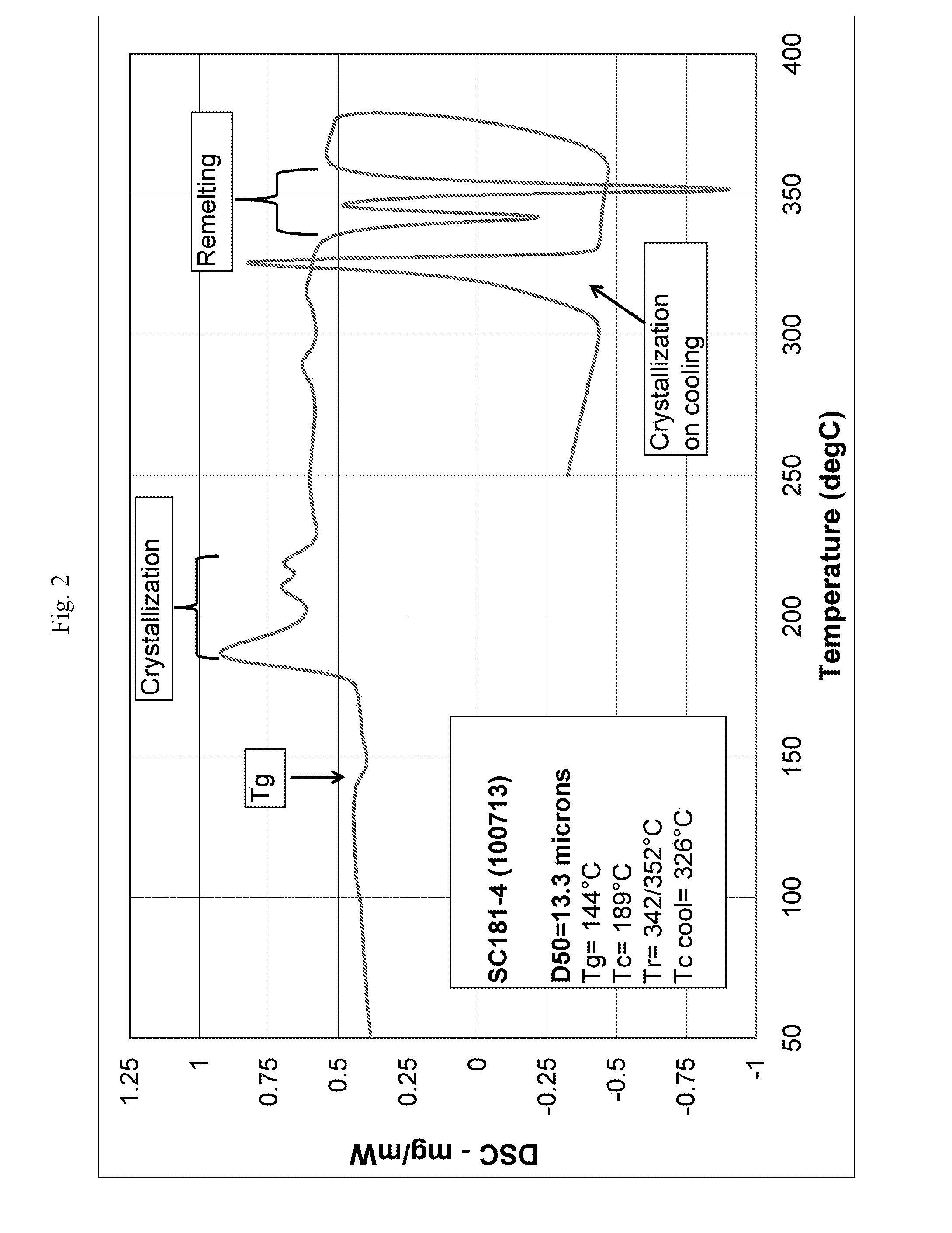
[0160]Glass frit: No. 25 (SC181-4); The specific surface area (Specific surface) of the glass frit measured by a BET method and the particle diameter of the glass frit measured by a laser diffraction-scattering method using MICROTRAC HRA9320-X100, manufactured by Nikkiso Co., Ltd., are shown in Table 6. With respect to glass frit No. 25, one obtained by grinding 100 g of the glass frit by means of a ball mill for 48 hours and subjecting the ground glass frit to sieve classification using a 400-mesh sieve was used. FIG. 4 shows scanning electron microscope (SEM) photomicrographs of glass frit No. 25 (SC181-4), taken at magnifications of (a) 1,000 times and (b) 500 times, wherein glass frit No. 25 was obtained after grinding by means of a ball mill for 48 ...


PUM

PropertyMeasurementUnit
mass ratioaaaaaaaaaa
temperatureaaaaaaaaaa
boundary temperatureaaaaaaaaaa

Abstract

A conductive paste including (A) conductive particles, (B) a glass frit containing substantially no lead, arsenic, tellurium, and antimony, and (C) a solvent. The glass frit (B) has a remelting temperature of 320 to 360° C., wherein the remelting temperature is indicated by a peak top of at least one endothermic peak having an endotherm of 20 J/g or more in a DSC curve as measured by a differential scanning calorimeter. The conductive paste can also include at least one metal oxide (D) selected from the group consisting of tin oxide, zinc oxide, indium oxide, and copper oxide. The glass frit (B) can further include (B-1) Ag2O, (B-2) V2O5, and (B-3) MoO3. The conductive paste can achieve binding at a relatively low temperature (such as 370° C. or lower) and maintains a bond strength at a relatively high temperature (such as 300 to 360° C.).

Description

FIELD OF THE INVENTION[0001]The present invention relates to a conductive paste comprising low melting-point glass which does not contain an injurious material, such as lead, and a method for producing a semiconductor device using the conductive paste.BACKGROUND ART[0002]A die attach material for bonding, for example, a silicon carbide (SiC) chip to a substrate, and a sealing material and a conductive paste for electronic parts, such as a ceramic package containing therein an integrated circuit device, and a display device, are desired to achieve bonding at relatively low temperatures, taking into consideration the properties of objects to be bonded or to be sealed which are extremely sensitive to heat. As a conductive paste which can achieve bonding at low temperatures, a composition comprising glass having a low melting point is used.[0003]Conventionally, as low melting-point glass, PbO—B2O3 glass having a low melting point has been known. Patent document 1 discloses, as glass hav...

Claims


Application Information

Patent Timeline
Patent Type & Authority Applications(United States)
IPC IPC(8): C03C8/24H01B1/16C03C4/14C03C3/12H01L23/00C09J9/02
CPCC03C8/24H01L24/83C09J9/02C03C4/14C03C3/122C03C3/127C03C2205/00H01B1/16H01L2224/83851H01L2224/83948H01L2924/10272C03C2204/00C03C3/125H01B1/22C03C8/02C03C8/18
Inventor DIETZ, RAYMONDPATELKA, MACIEJTRUMBLE, CATHY SHAWSAKAI, NORIYUKIYAMAGUCHI, HIROSHI
Owner NAMICS CORPORATION
Why Eureka
Try Eureka