Method for manufacturing device comprising inorganic/organic hybrid perovskite compound film and device comprising inorganic/organic hybrid perovskite compound film
a technology of inorganic/organic hybrid perovskite and compound film, which is applied in the direction of manufacturing tools, couplings, mechanical instruments, etc., can solve the problems of difficult to manufacture thin films having a dense and flat surface, and achieve excellent crystallinity, low cost, and simple process
- Summary
- Abstract
- Description
- Claims
- Application Information
AI Technical Summary
Benefits of technology
Problems solved by technology
Method used
Image
Examples
example 1
[0496]Perovskite Bonding
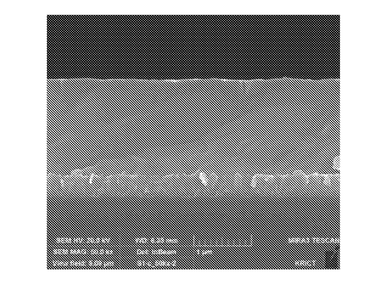
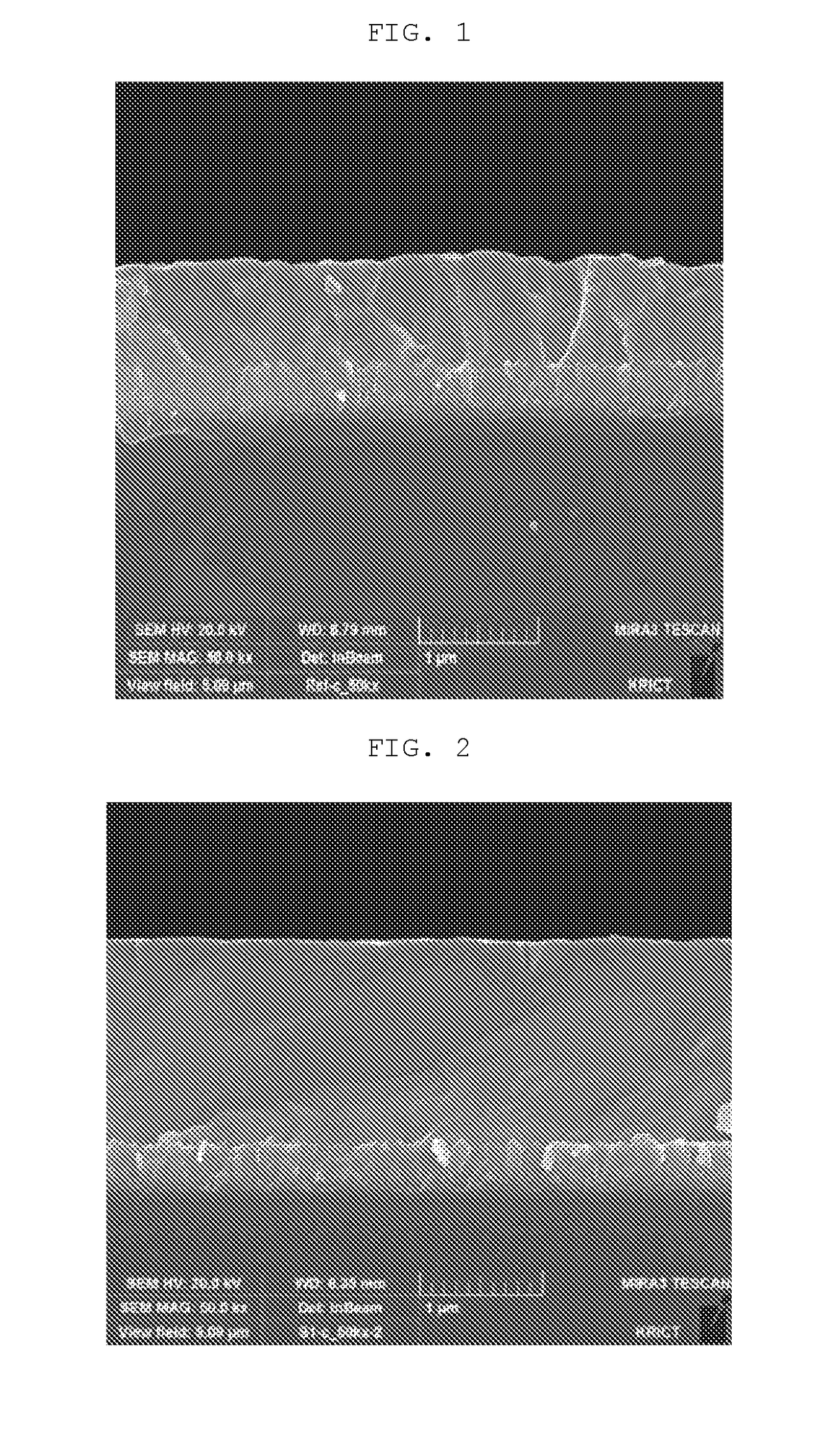
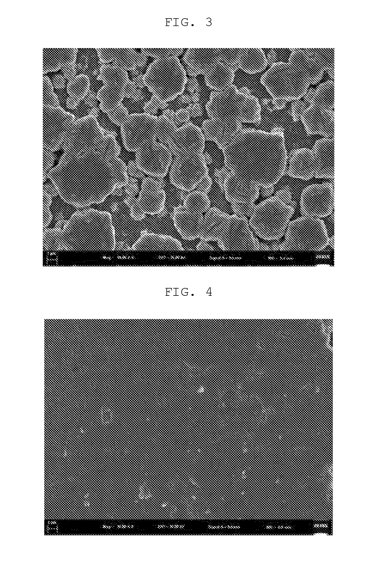
[0497]The CH3NH3PbI3 solution prepared in Preparation Example 1 was applied (injected) at one time to a rotation center of a glass substrate (FTO: F-doped SnO2, 8 ohms / cm2, Pilkington, hereinafter referred to as FTO substrate) coated with fluorine-containing tin oxide having a size of 25×25 mm, and spin-coated at 3000 rpm. After the spin coating was performed for 50 seconds, 1 mL of toluene, non-solvent, was applied (injected) at one time to the rotation center of the FTO substrate during spinning, and then, the spin coating was further performed for 5 seconds. After the spin coating was performed, the first surface layer, which was a perovskite compound film, was formed by processing at a temperature of 100 under normal pressure for 30 minutes. During the formation of the first surface layer, an ambient environment was maintained to a temperature of 25 and a relative humidity of 25%.
[0498]A second surface layer was formed on another FTO substrate in the same...
preparation example 2
[0502]Manufacture of Porous TiO2 Thin Film Substrate
[0503]A glass substrate coated with fluorine-containing tin oxide (FTO: F-doped SnO2, 8 ohms / cm2, Pilkington, hereinafter referred to as a FTO substrate (first electrode)) was cut into a size of 25×25 mm, and ends thereof were etched to partially remove the FTO.
[0504]A TiO2 dense film having a thickness of 50 nm as a metal oxide thin film was manufactured on the cut and partially etched FTO substrate by a spray pyrolysis method. The spray pyrolysis was performed by using a solution of TAA (titanium acetylacetonate):EtOH (1:9 v / v %), and the thickness was controlled by repeating a method of spraying the solution on the FTO substrate placed on a hot plate maintained at 450 for 3 seconds, followed by stopping the spraying for 10 seconds.
[0505]An ethyl cellulose solution in which 10% by weight of ethyl cellulose was dissolved in ethyl alcohol, was added to TiO2 powder having an average grain size (diameter) of 50 nm (prepared by hydrot...
preparation example 3
[0507]Manufacture of NiO Layer
[0508]A glass substrate coated with fluorine-containing tin oxide (FTO: F-doped SnO2, 8 ohms / cm2, Pilkington, hereinafter referred to as a FTO substrate (first electrode)) was cut into a size of 25×25 mm, and then, the remaining FTO except for portions where four rectangular electrodes each having a size of 4 mm×20 mm were disposed was removed so that the four rectangular electrodes were disposed.
[0509]A NiO dense film having a thickness of 50 nm as a metal oxide thin film was manufactured on the cut and partially etched FTO substrate. The NiO dense film was manufactured by spin coating a NiO solution on the FTO substrate, followed by heat treatment. The NiO solution was prepared by adding 0.0589 g of nickel nitrate hexahydrate and 12.5 μl of monoethanolamine to 2 ml of ethanol and stirring at 70 for 4 hours. This solution was coated on the FTO substrate prepared above at 3000 rpm, and then heat-treated at 250□ for 30 minutes.
PUM
 Abstract
Description
Claims
Application Information


