Photonic and electric devices on a common layer

a technology of electric devices and photonic modulators, applied in semiconductor lasers, non-linear optics, instruments, etc., can solve the problems of difficult integration with electronic devices and circuits of group iii-n, limiting the growth thickness of photonic waveguide layers, and relatively high loss, so as to achieve the effect of significantly improving the efficiency of photonic modulators and lasers

Active Publication Date: 2019-11-14
RAYTHEON BBN TECH CORP +1
View PDF7 Cites 11 Cited by
  • Summary
  • Abstract
  • Description
  • Claims
  • Application Information

AI Technical Summary

Benefits of technology

[0047]Thus, with such an arrangement, the efficiency of a photonic modulator and laser can be significantly improved.

Problems solved by technology

However, a major challenge has been the crystalline lattice mismatch between the photonic waveguiding layer and the underneath cladding layer which results in the generation of high density of crystalline dislocations limiting the growth thickness of the photonic waveguiding layer.
While Approach (2) can provide a viable platform for photonic devices, its integration with Group III-N electronic devices and circuits is difficult.
Approach (3) can yield the single crystalline material in the growth direction; in the lateral direction, it is amorphous or polycrystalline resulting in relatively high loss and electronic device integration difficulties.
In addition, Silicon (Si) has a larger refractive index than GaN and AlGaN, and so it cannot be an effective optical cladding layer for GaN and AlGaN in many applications.
For such devices based on III-Nitrides materials employing Aluminum Nitride (AlN), Gallium Nitride (GaN) and / or Indium Nitride (InN) and their respective ternary or quaternary alloys, maximizing this difference unfortunately leads to layers for the photonic waveguiding layer and cladding to be highly structurally mismatched thus limiting the thicknesses of these layers to be much thinner than desired / required to avoid any significant generation of lattice defects and dislocations in the device.
This is presently a major challenge for such devices to be built on Group III-Nitride materials.
However, some major challenge limits their efficiency as well as their compatibility for either in-plane or out-of-plane operation.
These challenges include:1—The large crystalline lattice mismatch between the stack of quantum well layers forming the modulator, which set a limit on increasing the layer thickness as well as reduces the efficiency of the quantum well for interaction with light.
This becomes particularly troublesome when going to wavelengths longer than blue (e.g. green) which requires thicker quantum wells, thereby efficiency in green wavelength lasers and modulators can drop quite rapidly.2—For in-plane waveguide modulators as well as in-plane lasers, a fundamental requirement for a photonic waveguiding layer is to have a refractive index larger than the cladding material, while being closely lattice matched to the underneath or upper material cladding which is also crystalline.
However, a major challenge has been the crystalline lattice mismatch between the photonic waveguiding layer and the cladding material which limits the growth thickness of the photonic waveguiding layer to avoid onset of dislocation generation in the crystal degrading the overall performance of the modulator and lasers.
For out-of-plane modulators and vertical emitting lasers a stack of distributed Bragg reflector (DBR) layers is needed to vertically confine the light, the crystalline lattice mismatch between the layer stacks sets a limit on the thickness of the DBR layers, such that increasing the layer thickness reduces the material quality and results in large optical absorption and scattering.
Therefore, making DBR layers with desired thickness becomes quite challenging, particularly as the operation wavelength increases.
In prior art making high efficient lasers at longer wavelengths (˜500 nm and above) based on Group III-Nitride structures has been quite challenging due to the crystalline lattice mismatch and limited thickness of the DBR.

Method used


Image

  • Photonic and electric devices on a common layer
  • Photonic and electric devices on a common layer
  • Photonic and electric devices on a common layer

Examples


Embodiment Construction

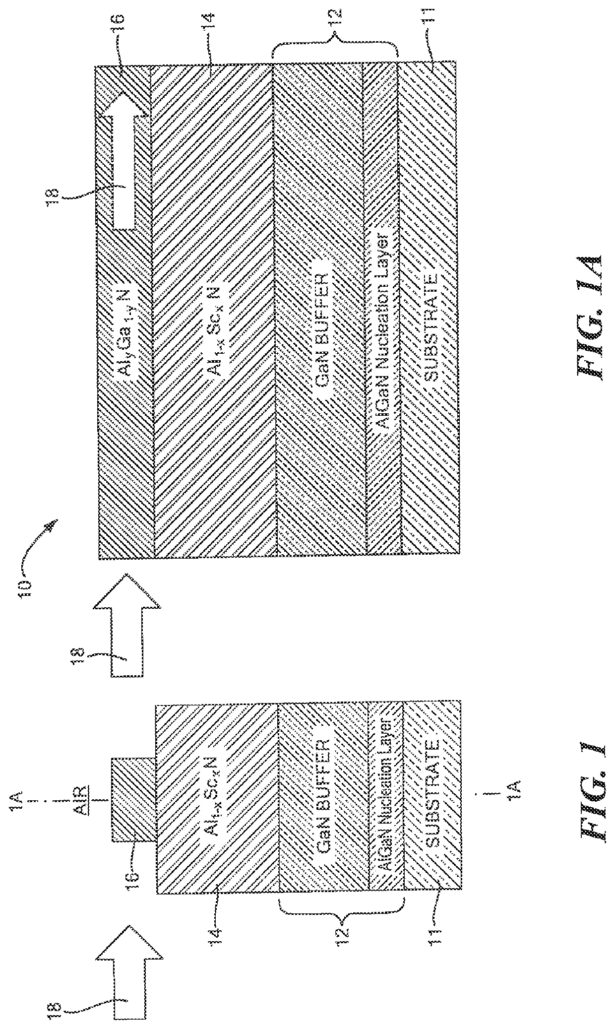
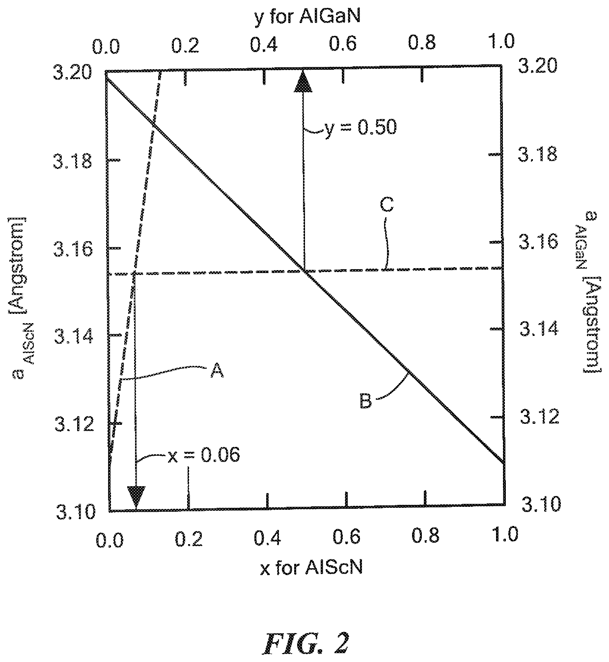
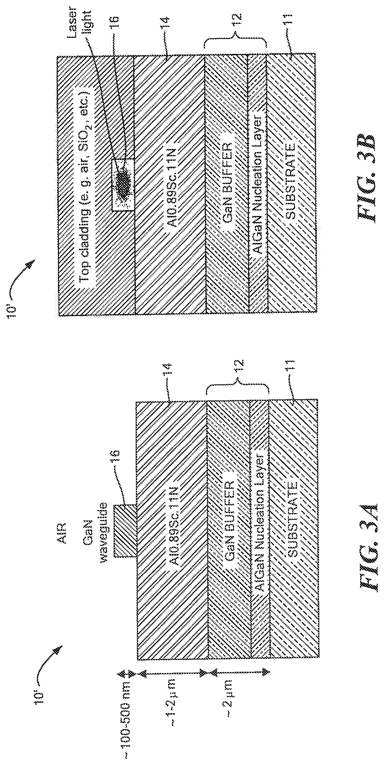
[0064]Referring now to FIGS. 1 and 1A, a photonic device 10, here a photonic waveguide, is shown having: a substrate 11, here a single crystal substrate, for example, Silicon Carbide (SiC), an AlGaN nucleation layer / GaN buffer layer 12 on the substrate 11, the AlGaN nucleation layer portion of layer 12 serves to allow the GaN buffer above it be fully relaxed. This nucleation layer / buffer layer 12 accommodates all the mismatching of III-N layers to the substrate, here for example the SiC substrate 11; a cladding layer 14, here Aluminum Scandium Nitride (Al1-xScxN), formed on an upper surface of the AlGaN nucleation layer / GaN buffer layer 12 formed in a manner to be described below; and a photonic waveguiding layer 16, here a Group III-Nitride single crystal compound, here Aluminum Gallium Nitride (AlyGa1-yN), formed by epitaxial growth it being noted that the values of 01-xScxN) cladding layer 14 and the Aluminum Gallium Nitride (AlyGa1-yN) photonic waveguiding layer 16; it being not...


PUM

PropertyMeasurementUnit
thicknessaaaaaaaaaa
thicknessaaaaaaaaaa
operation wavelengthaaaaaaaaaa

Abstract

Photonic devices having Al1-xScxN and AlyGa1-yN materials, where Al is Aluminum, Sc is Scandium, Ga is Gallium, and N is Nitrogen and where 0<x≤0.45 and 0≤y≤1.

Description

CROSS REFERENCE TO RELATED APPLICATION[0001]This application claims priority from U.S. Provisional Patent Application Ser. No. 62 / 670,261, filed on May 11, 2018 which is incorporated herein by reference in its entirety.TECHNICAL FIELD[0002]This disclosure relates generally to photonic devices. The disclosure also relates to structures adapted to have a photonic device and semiconductor electronic device disposed on a common single crystal layer. The disclosure also relates to structures having photonic devices and Group III-N semiconductors.BACKGROUND OF THE INVENTION[0003]As is known in the art, photonic devices are used to: generate photons, as with a laser; modify the propagation of photons, as with an amplifier, modulator, switch, or electro-optical device; or, detect photons, as with a photon detector. As is also known in the art, many of these photonic devices are formed using a vertical stack of horizontally disposed layers of different materials and include: a photonic waveg...

Claims


Application Information

Patent Timeline
Patent Type & Authority Applications(United States)
IPC IPC(8): G02B6/122H01L29/20H01L29/778H01S5/343
CPCG02B2006/12142H01L29/2003G02B2006/1213H01L29/778G02B2006/12121H01S5/34333G02B2006/12035G02B6/1225H01L21/02521H01L21/0254H01L21/02378H01L21/02439H01L21/02458H01L21/02505H01L29/7786H01L29/201H01L29/66462H01L29/0843H01S2301/173H01S5/3214H01S5/04257H01S5/18361G02F1/01708G02F1/01716H01S5/04253H01S5/18347H01S5/22H01S5/3211G02B6/122G02B6/12G02F2202/108H01L29/7783H01S5/125H01S5/343
Inventor SOLTANI, MOHAMMADCHUMBES, EDUARDO M.
Owner RAYTHEON BBN TECH CORP
Why Eureka
Try Eureka