

Method for preparing film micro-optical structure based on photolithography and chemomechanical polishing
a micro-optical structure and photolithography technology, applied in the field of photolithography and chemomechanical polishing, can solve the problems of limited processing efficiency, difficult preparation of high-quality structures in millimeter or even centimeter levels, and inability to meet the requirements of micro-optical integration on-chip
- Summary
- Abstract
- Description
- Claims
- Application Information
AI Technical Summary
Benefits of technology
Problems solved by technology
Method used
Image

Examples
embodiment 1
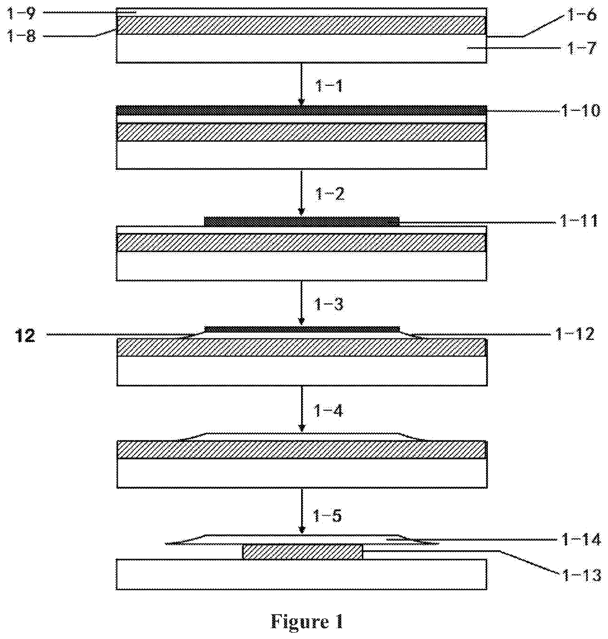
[0047]In the first embodiment of the present invention as shown in FIG. 1, an optical whispering gallery mode microdisk cavity on-chip is prepared by femtosecond laser combined with chemical mechanical polishing in the present invention. The method of the present invention is now illustrated by taking a lithium niobate single crystal film on-chip as an example. As can be seen from the figure, the method for preparing an optical whispering gallery mode microcavity on-chip by femtosecond laser combined with chemical mechanical polishing comprises the following five steps:
[0048](1-1) Coating Cr metal film on surface: Lithium niobate single crystal film on-chip sample 1-6 with size of 3 mm×4 mm×1 mm is taken and is composed of a about 1 mm thick substrate 1-7, a 2 μm thick SiO2 film 1-8 on the substrate and a 900 nm thick LiNbO3 film 1-9 on the SiO2 film. A 900 nm Cr metal film 1-10 is coated on the surface of LiNbO3 film 1-9.
[0049](1-2) Femtosecond laser ablation: the above coated samp...
embodiment 2
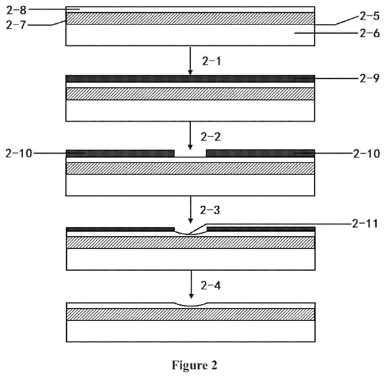
[0053]In the second embodiment of the present invention as shown in FIG. 2, a saddle coupling region on-chip is prepared by femtosecond laser combined with chemical mechanical polishing in the present invention. The method of the present invention is now illustrated by taking a lithium niobate single crystal film on-chip as an example. As can be seen from the figure, the method for preparing a saddle coupling region on-chip by femtosecond laser combined with chemical mechanical polishing comprises the following four steps:
[0054](2-1) Coating Cr metal film on surface: Lithium niobate single crystal film on-chip sample 2-5 with size of 3 mm×4 mm×1 mm is taken and is composed of a about 1 mm thick substrate 2-6, a 2 μm thick SiO2 film 2-7 on the substrate and a 900 nm thick LiNbO3 film 2-8 on the SiO2 film. A 900 nm Cr metal film 2-9 is coated on the surface of LiNbO3 film 2-8.
[0055](2-2) Femtosecond laser ablation: the above coated sample is washed with anhydrous ethanol and fixed ont...
embodiment 3
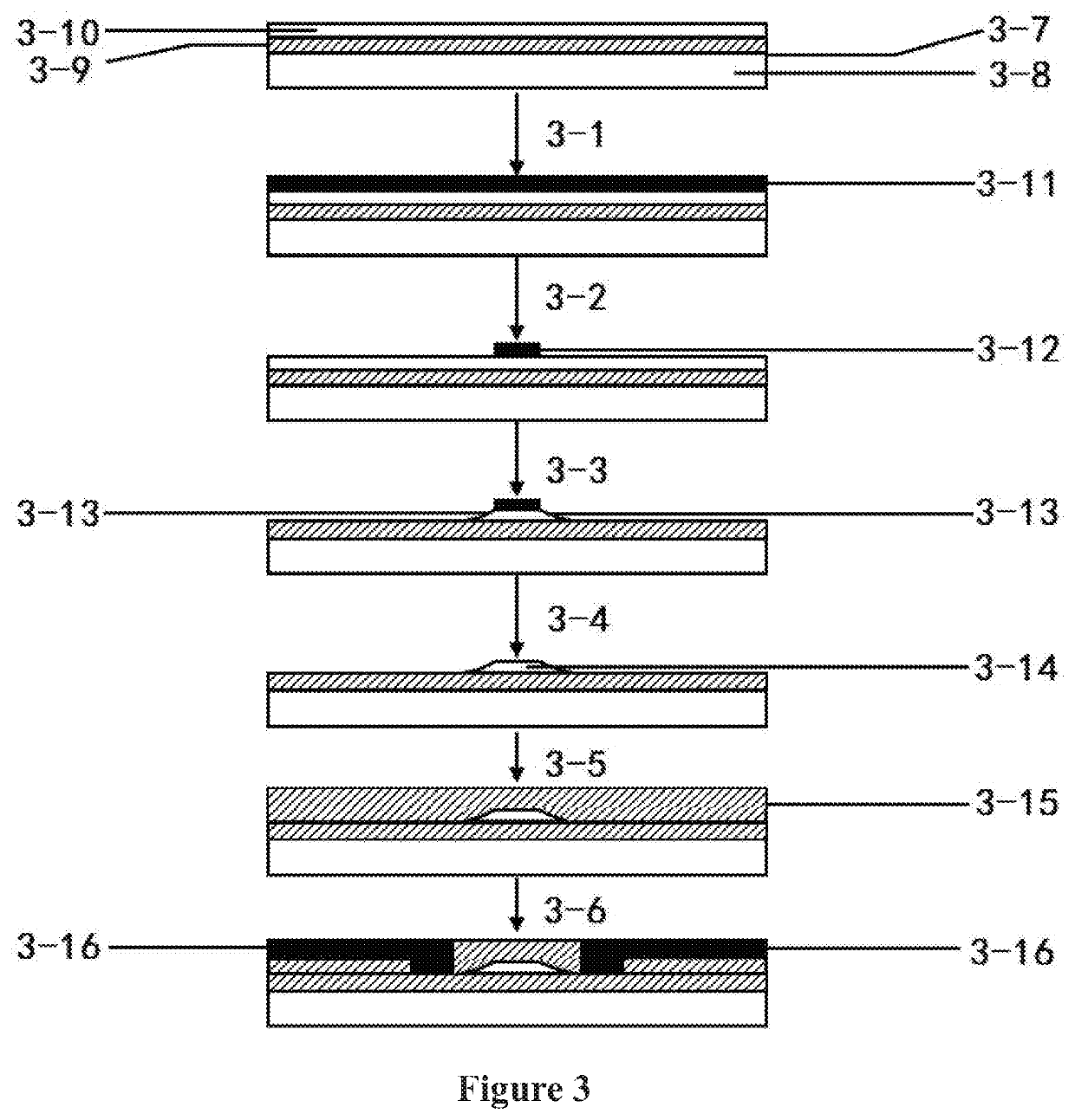
[0058]In the third embodiment of the present invention as shown in FIG. 3, a low-loss electro-optic tunable waveguide on-chip is prepared by femtosecond laser combined with chemical mechanical polishing in the present invention. The method of the present invention is now illustrated by taking a lithium niobate single crystal film on-chip as an example. As can be seen from the figure, the method for preparing a low-loss electro-optic tunable waveguide on-chip by femtosecond laser combined with chemical mechanical polishing comprises the following six steps:
[0059](3-1) Coating Cr metal film on surface: Lithium niobate single crystal film on-chip sample 3-7 with size of 3 mm×4 mm×1 mm is taken and is composed of a about 1 mm thick substrate 3-8, a 2 μm thick SiO2 film 3-9 on the substrate and a 900 nm thick LiNbO3 film 3-10 on the SiO2 film. A 900 nm Cr metal film 3-11 is coated on the surface of LiNbO3 film 3-10.
[0060](3-2) Femtosecond laser ablation: the above coated sample is washed...
PUM
| Property | Measurement | Unit |
|---|---|---|
| size | aaaaa | aaaaa |
| size | aaaaa | aaaaa |
| size | aaaaa | aaaaa |
Abstract
Description
Claims
Application Information