Composition for depositing silicon-containing thin film containing bis(aminosilyl)alkylamine compound and method for manufacturing silicon-containing thin film using the same

a technology of bis(aminosilyl)alkylamine and compound, which is applied in the direction of silicon compounds, silicon oxides, organic chemistry, etc., can solve the problems of physical and electric properties, and achieve the effects of high volatility, excellent thermal stability, and high purity and durability

Active Publication Date: 2020-04-09
DNF
View PDF0 Cites 1 Cited by
  • Summary
  • Abstract
  • Description
  • Claims
  • Application Information

AI Technical Summary

Benefits of technology

[0029]A composition for depositing a silicon-containing thin film contains a bis(aminosilyl)alkylamine compound which is a liquid at room temperate and has high volatility and excellent thermal stability as a precursor, such that a high-quality silicon-containing thin film having a high purity and durability may be provided under lower plasma power and film formation temperature conditions.
[0030]Further, in a method for manufacturing a silicon-containing thin film using the composition for depositing a silicon-containing thin film according to the present invention, excellent thermal stability and deposition rate, and excellent stress intensity may be implemented even under a low film formation temperature condition, and in a silicon-containing thin film manufactured thereby, contents of impurities such as carbon, oxygen, and hydrogen are minimized, thereby making it possible to manufacture a silicon-containing thin film having a high purity, excellent physical and electrical properties, excellent resistance against hydrogen fluoride, an excellent water vapor transmission rate, and an excellent step coverage.

Problems solved by technology

Therefore, a high-temperature process (600° C. or more) using an existing silicon precursor, a step coverage, etching properties, and physical and electric properties of the thin film have become problems, such that the development of a novel more excellent silicon precursor and a method for forming a thin film have been studied.

Method used


Image

  • Composition for depositing silicon-containing thin film containing bis(aminosilyl)alkylamine compound and method for manufacturing silicon-containing thin film using the same
  • Composition for depositing silicon-containing thin film containing bis(aminosilyl)alkylamine compound and method for manufacturing silicon-containing thin film using the same
  • Composition for depositing silicon-containing thin film containing bis(aminosilyl)alkylamine compound and method for manufacturing silicon-containing thin film using the same

Examples


example 2

[Example 2] Preparation of Bis(ethylmethylaminosilyl)methylamine

[0090]

[0091]Under an anhydrous and inert atmosphere, after putting dichlorosilane (SiH2Cl2, 360 g (3.56 mol)) and n-pentane (3,202 g (27.79 mol)) into a 5000 mL flame-dried Sus reactor (a high-pressure reactor) and slowly adding methylamine (CH3NH2, 210 g (6.77 mol)) thereto while maintaining a temperature at −25° C., the mixture was stirred for 3 hours, and methylamine hydrochloride ((CH3)NH3C1)) was removed by filtration. While stirring a recovered bischlorolsilylamine ((SiH2C1)2N(CH3)) solution with n-pentane and maintaining a temperature at −25° C., ethylmethylamine ((CH3CH2)(CH3)NH), 421 g (7.13 mol)) was slowly added thereto. After the addition was completed, the reaction solution was slowly heated to room temperature and stirred at room temperature for 6 hours. After removing ethylmethylamine hydrochloride ((CH3CH2)(CH3)NH2Cl), white) formed by filtering the resultant, a filtrate was obtained. A solvent was remov...

example 3

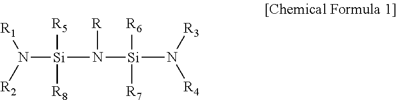
[Example 3] Manufacturing of Silicon Oxide Thin film by PEALD using Bis(ethylmethylaminosilyl)methylamine

[0093]Film was formed using the bis(ethylmethylaminosilyl)methyl amine compound prepared in Example 2 according to the present invention as a composition for forming a silicon oxide film in a general plasma enhanced atomic layer deposition (PEALD) apparatus using a plasma enhanced atomic layer deposition (PEALD) method known in the art.

[0094]As a reaction gas, nitrous oxide was used together with plasma, and nitrogen corresponding to an inert gas was used for purging. The film was formed at reaction gas and plasma time of 0.5 seconds. A specific method for depositing a silicon oxide thin film was illustrated in Table 1.

[0095]A result obtained by analyzing the manufactured silicon oxide thin film was illustrated in Table 2, and a result obtained by analyzing the deposited film using infrared spectroscopy was illustrated in FIG. 3.

examples 4 and 5

[Examples 4 and 5] Manufacturing of Silicon Oxide Thin film by PEALD using Bis(ethylmethylaminosilyl)methylamine

[0096]Silicon oxide thin films were manufactured in the same manner as in Example 3 except for changing deposition conditions illustrated in the following Table 1 in Example 3, results obtained by analyzing the manufactured silicon oxide thin film were illustrated in the following Table 2, and results obtained by analyzing the deposited film using the infrared spectroscopy were illustrated in FIG. 3.

TABLE 1Deposition Conditions of Silicon Oxide Thin Film by PEALDReaction GasReactionNo. ofTemperaturePrecursorPurgeand PlasmaGas PurgeDepositionof SubstrateHeatingInjectionFlow RateTimeFlow RateRFTimeTimeFlow RateProcess(° C.)Temperature (° C.)Time (sec)(sccm)(sec)(sccm)Power (W)(sec)(sec)(sccm)CycleTime (sec)Example 390650.16000.48004000.50.1300614675Example 490650.16000.48004000.70.1300603784Example 590650.16000.48004000.90.1300603905

TABLE 2Evaluation of Properties of Silicon...


PUM

PropertyMeasurementUnit
temperatureaaaaaaaaaa
plasma poweraaaaaaaaaa
poweraaaaaaaaaa

Abstract

Provided are a composition for depositing a silicon-containing thin film containing a bis(aminosilyl)alkylamine compound and a method for manufacturing a silicon-containing thin film using the same, and more particularly, a composition for depositing a silicon-containing thin film, containing the bis(aminosilyl)alkylamine compound capable of being usefully used as a precursor of the silicon-containing thin film, and a method for manufacturing a silicon-containing thin film using the same.

Description

TECHNICAL FIELD[0001]The present invention relates to a composition for depositing a silicon-containing thin film and a method for manufacturing a silicon-containing thin film using the same, and more particularly, to a composition for depositing a silicon-containing thin film, containing a specific compound, a bis(aminosilyl)alkylamine compound as a precursor for depositing a thin film, and a method for manufacturing a silicon-containing thin film using the same.BACKGROUND ART[0002]A silicon-containing thin film is manufactured through various deposition processes in a semiconductor field to thereby be manufactured in various forms such as a silicon film, a silicon oxide film, a silicon nitride film, a silicon carbonitride film, and a silicon oxynitride film, and an application field of the silicon-containing thin film may be wide.[0003]Particularly, since the silicon oxide film and the silicon nitride film have a significantly excellent barrier property and oxidation resistance, t...

Claims


Application Information

Patent Timeline
Patent Type & Authority Applications(United States)
IPC IPC(8): H01L21/02C09D1/00C01B33/18C01B21/068C07F7/10C23C16/455C23C16/50C23C16/40C23C16/34C23C16/30C23C16/36C23C16/32
CPCC23C16/308C01B33/183H01L21/02167C23C16/325C23C16/4554H01L21/0228C23C16/401C23C16/345H01L21/02164H01L21/02271H01L21/02208C01B21/068H01L21/0214H01L21/02126H01L21/0217C23C16/50C09D1/00C07F7/10C23C16/36H01L21/02274H01L21/02219C23C16/45542C23C16/45553C09D183/16C23C16/24C09D4/00H01L21/324
Inventor KIM, SUNG GIPARK, JEONG JOOPARK, JOONG JINJANG, SE JINYANG, BYEONG-ILLEE, SANG-DOLEE, SAM DONGLEE, SANG ICKKIM, MYONG WOON
Owner DNF
Why Eureka
Try Eureka