

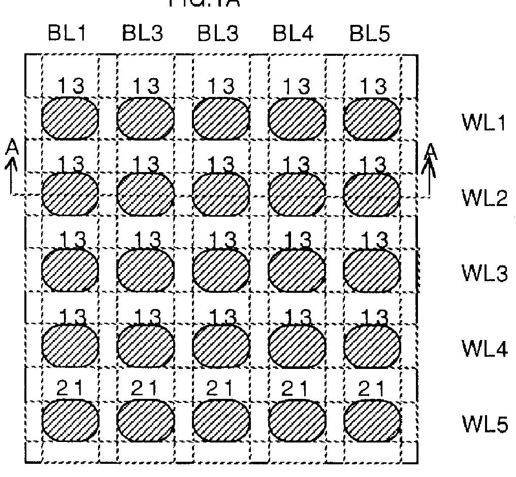
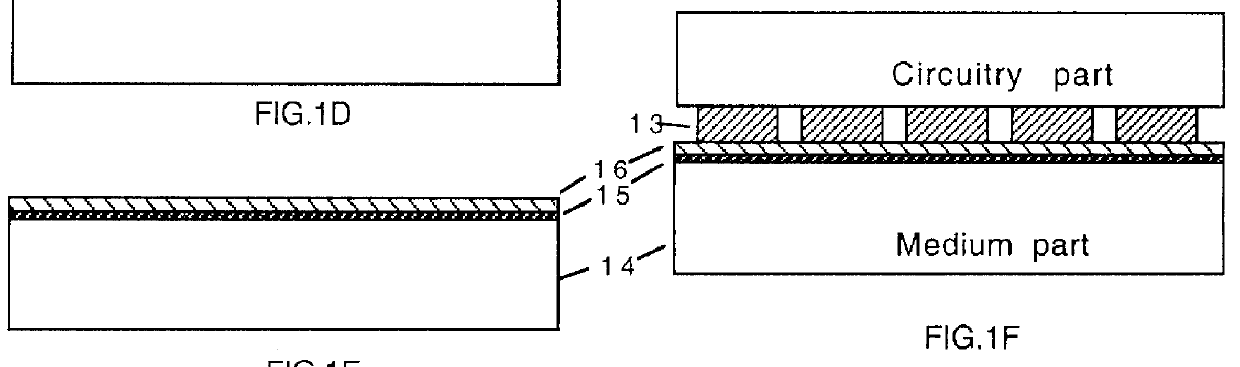
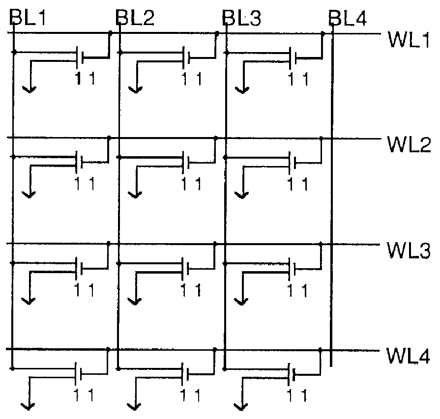
Two-parts ferroelectric RAM
a ferroelectric ram and ram technology, applied in the field of ferroelectric rams, can solve the problems of affecting the use of other nonvolatile memory devices, affecting the production efficiency of the device, so as to facilitate the manufacture of the device, reduce the number of steps, and increase the total yield
- Summary
- Abstract
- Description
- Claims
- Application Information
AI Technical Summary
Benefits of technology
Problems solved by technology
Method used
Image

Examples
example 2
(For Temporary as Well as Permanent Connection)
Same as example 1, except that the photosensitivity of the polyisoprene is utilized for the curing (crosslinking) of the whole layer, not for photolithography. After the spin coating and the evaporation of the xylene, as in example 1, the whole layer (with no mask) is exposed in UV light for curing. After curing, an additional photolithography step is carried out to pattern the layer into an array of pads. For this a silicone containing photoresist layer should be applied on top of the polyaniline / elastomer blend layer. By means of photolithography and an additional RIE (Reaction Ion Etch) step, we can pattern the polyaniline / elastomer layer into an array of pads as we desired. With the advantage of RIE, we can get better profile of the pads, on the cost of an additional fabrication step.
example 3
(For Temporary as Well as Permanent Connection)
Similar to example 2, except the polyisoprene not necessarily be photosensitive. No sensitizer (such as 2,6-Bis(4-azidobenzylidene)4-methylcyclo-hexanone) will be added. Heat curing is employed in place of UV light curing.
example 4
(For Temporary as Well as Permanent Connection)
For the conductive conjugate polymer, we can choose polyaniline protonated with camphorsulfonic acid. Emeraldine base form of polyaniline (PANI) is mixed with camphorsulfonic acid (CSA), in molar ratio of CSA to polyaniline unit=0.5, using an agate mortar and pestle in nitrogen atmosphere. An appropriate quantity of the resulting mixture is placed into m-cresol, treated in an ultrasonic bath for 48 hours at 50.degree. C. The PANI complex dissolves to give a viscous deep green solution. This PANI-CSA complex is chosen as the conductive conjugate polymer. For the elastomer, we can choose the one part blocked polyurethane (such as the .RTM.Mondur, produced by the Miles Chemical Corp. Pittsburgh, Pa. 15205). Both these two components are soluble in m-cresol. Solution of these two components in m-cresol, with PANI-CSA to polyurethane ratio about 1:10, is mixed and spin-coated on the surface of the circuitry part. After evaporation of the sol...
PUM
| Property | Measurement | Unit |
|---|---|---|
| Fraction | aaaaa | aaaaa |
| Angle | aaaaa | aaaaa |
| Temperature | aaaaa | aaaaa |
Abstract
Description
Claims
Application Information