Optical semiconductor device

a semiconductor and optical technology, applied in semiconductor lasers, pulse techniques, instruments, etc., can solve the problems of blue lasers that are difficult to obtain for practical use, high threshold values of optical semiconductor devices, and difficult to achieve a suitable material system for use, etc., to achieve easy population inversion, excellent characteristics, and simple construction

Inactive Publication Date: 2000-03-28
KK TOSHIBA
View PDF5 Cites 73 Cited by
  • Summary
  • Abstract
  • Description
  • Claims
  • Application Information

AI Technical Summary

Benefits of technology

An object of the present invention is to provide a GaN-based semiconductor laser for obtaining laser oscillation at a low threshold value by enabling easy population inversion. Another object of the present invention is to provide an optical bistable element having excellent characteristics. A further object of the present invention is to provide a semiconductor laser having a simple construction which can be made compact and shows high speed switching characteristics of circularly polarized light applicable to optical communication by phase shift keying (PSK).

Problems solved by technology

However, these optical semiconductor devices have respective problems as shown in the following description.
However, in this material system, the electron effective mass is large so that it is hard to cause population inversion.
Accordingly, this material system has disadvantages in that a threshold value is essentially high in comparison with the conventional material system.
Therefore, a blue laser is difficult to obtain for practical use.
However, in this element structure, a carrier relaxation is caused by LO phonons at a very high speed so that it is hard to cause population inversion.
Therefore, an intersubband transition laser is difficult to obtain for practical use.
However, a bistable element having excellent characteristics has not been realized yet.
However, a switching speed of a magneto-optic element, a liquid crystal or an electro-optic element used in phase control of a laser beam is generally low.
Therefore, it is difficult to have a wide band width practical communication system by using phase shift keying (PSK).
Therefore, the construction of the device is large-sized.
Further, when a polarizing direction is modulated, the device becomes complicated and large-sized.
Accordingly, it was difficult to make the device compact and to reduce the cost of the device.
However, because the response of magnetization inversion by the external magnetic field in the magnetic material is not high it is hard to modulate the circularly polarized light at high speed.

Method used


Image

  • Optical semiconductor device
  • Optical semiconductor device
  • Optical semiconductor device

Examples


example 1

FIG. 6 shows a cross-sectional view of the semiconductor laser in this Example. In FIG. 6, an undoped GaN layer 102, an n-type GaN contact layer 103, an n-type AlGaN cladding layer 104, an undoped GaN optical guide layer 105, a quantum well layer 106 constructed by InGaN / InGaN, a p-type GaN optical guide layer 107, a p-type AlGaN cladding layer 108, and a p-type GaN contact layer 109 are formed in this order on a sapphire substrate 101. Strain of 1% is introduced to the quantum well layer 106. An electric current is confined by forming a mesa structure of 10 .mu.m in width. A CoFe ferromagnetic layer 110 is formed on the p-type GaN contact layer 109. Further, an electrode 111 is formed on the exposed n-type GaN contact layer 103 and an electrode 112 is formed on the CoFe ferromagnetic layer 110.

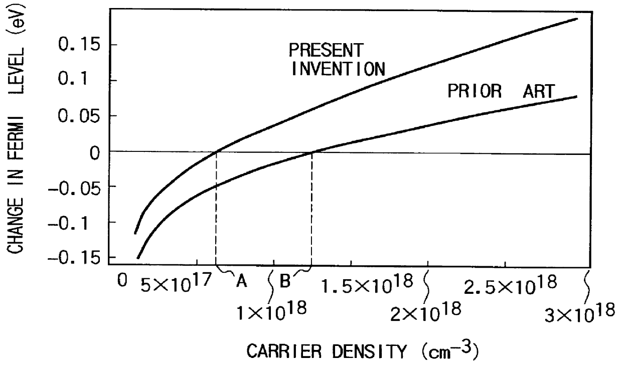
The threshold current density of this semiconductor laser is 1.5 kA / cm.sup.2. This threshold current density is greatly reduced in comparison with 3 kA / cm.sup.2 in the conventional semiconduc...

example 2

FIG. 7 shows a cross-sectional view of the inter subband transition type semiconductor laser in this Example. In FIG. 7, an n-type InP cladding layer 202, an InGaAs / InGaAsP quantum well layer 203, an InGaAsP waveguide layer 204 and an n-type InP cladding layer 205 are formed in this order on an n-type InP substrate 201. An n-type contact layer 206 and a CoFe ferromagnetic layer 207 are formed on the n-type InP cladding layer 205. Further, an electrode 208 is formed on the CoFe ferromagnetic layer 207 and an electrode 209 is formed on the rear surface of the n-type InP substrate 201.

Although this semiconductor laser has a simple construction, oscillation is obtained at a threshold current density of 5 kA / cm.sup.2. No oscillation can be conventionally obtained unless the semiconductor laser has a complicated structure. Accordingly, it is known from this that the threshold value can be greatly reduced in the semiconductor laser of FIG. 7.

example 3

FIG. 8 shows a cross-sectional view of the optically pumped bistable semiconductor laser in this Example. This semiconductor laser has a structure similar to that of FIG. 6. Namely, an undoped GaN layer 102, an n-type GaN contact layer 103, an n-type AlGaN cladding layer 104, an undoped GaN optical guide layer 105, a quantum well layer 106 constructed by InGaN / InGaN, a p-type GaN optical guide layer 107, a p-type AlGaN cladding layer 108 and a p-type GaN contact layer 109 are formed in this order on a sapphire substrate 101. Strain of 1% is introduced to the quantum well layer 106. A generated carrier is confined by forming a mesa structure of 10 .mu.m in width. However, this structure differs from that in FIG. 6 in that a magnetic layer and an electrode are not formed on the contact layers.

When circularly polarized pumping light is inputted from a light source 120 to this laser, oscillation is started with a light output corresponding to 3 kA / cm.sup.2 in carrier density. The oscill...


PUM

PropertyMeasurementUnit
widthaaaaaaaaaa
ferromagneticaaaaaaaaaa
magnetizationaaaaaaaaaa

Abstract

An optical semiconductor device has a structure in which a semiconductor active layer is sandwiched by a p-type semiconductor cladding layer and an n-type semiconductor cladding layer and a p-type contact layer is formed on the p-type semiconductor cladding layer side and an n-type contact layer is formed on the n-type semiconductor cladding layer side, wherein two ferromagnetic layers are formed on the n-type contact layer and two ferromagnetic layers are formed on the p-type contact layer. Magnetization directions of a pair of ferromagnetic layers vertically opposed to each other are set to be parallel to each other, and the magnetization directions of adjacent ferromagnetic layers are inverted to each other.

Description

The present invention relates to an optical semiconductor device.Recently, optical semiconductor devices have been developed. However, these optical semiconductor devices have respective problems as shown in the following description.For example, a blue light source has been vigorously developed to become the light source for a display and the next generation DVD. A GaN-based semiconductor has particularly attracted attention since its emission wavelength can be shortened to an ultraviolet ray. However, in this material system, the electron effective mass is large so that it is hard to cause population inversion. Accordingly, this material system has disadvantages in that a threshold value is essentially high in comparison with the conventional material system. Therefore, a blue laser is difficult to obtain for practical use.A semiconductor laser using intersubband transition within a conduction band instead of interband transition conventionally utilized has attracted attention as ...

Claims


Application Information

Patent Timeline
Patent Type & Authority Patents(United States)
IPC IPC(8): H01S5/04H01S5/042H01S5/00G02F3/02G02F3/00H01S5/323H01S5/06
CPCB82Y20/00H01S5/041H01S5/0425G02F3/026H01S5/0607H01S5/32341H01S5/3404H01S2301/173H01S5/04257
Inventor KAMIGUCHI, YUZOHIRAYAMA, YUZOSAHASHI, MASASHI
Owner KK TOSHIBA
Why Eureka
Try Eureka