Integrated, multi-chip, thermally conductive packaging device and methodology

a packaging device and thermally conductive technology, applied in semiconductor devices, semiconductor/solid-state device details, electrical apparatus, etc., can solve the problems of affecting the performance of the devi

Inactive Publication Date: 2000-06-13
GOOGLE LLC
View PDF25 Cites 71 Cited by
  • Summary
  • Abstract
  • Description
  • Claims
  • Application Information

AI Technical Summary

Problems solved by technology

However, as is well-known, power dissipation from transistors is at a maximum during switching (and, ideally, zero when a transistor is fully turned on or off).
Higher operating temperatures can only be utilized to a limited degree in increasing heat dissipation since semiconductor devices will degrade in performance or be destroyed if temperature limits are exceeded.
Thus, for high-performance digital switching circuits (and, of course, analog and power circuits, as well) heat dissipation is a limitation on performance and, as a practical matter, on integration density, forcing a trade-off between manufacturing costs and potential performance while limiting improvements in both.
Such cooling systems are, themselves, very expensive in terms of both manufacturing costs and integration with complex and compact electronic systems, limiting miniaturization and imposing at least two additional failure modes.
Specifically, such cooling systems are generally of a geometry and configuration which displaces or prevents the significant utilization of convection or radiant heat transfer and, of course, are subject to malfunction which would allow temperature limits to be exceeded very quickly.
Therefore, cooling systems which rely on a large temperature differential between chips and coolant fluid for efficiency may cause wide temperature excursions and thermal cycling of chips which may also degrade the structures therein (e.g. by metal fatigue or migration and internal semiconductor stresses which may be relieved by formation of crystal dislocations that may thereafter trap charge, cause leakage, etc.).
However, increased density of package mounting is subject to the same problems of heat dissipation at the level of the substrate area as discussed above in connection with chip area.
Further, vertical mounting of chips generally provides less support and structural robustness of the chip mounting structure.
In this regard, the length of heat conduction through the heat sink, itself, must also be considered in the efficiency of the design thereof together with package mounting density and maximum or even adequate thermal performance is seldom consistent with maximum electrical performance and compactness.
Additionally, heat transfer from the edge of a chip is necessarily poor and generally requires conduction of heat through the semiconductor substrate of the chips.
Transfer of heat to such a heat sink is also problematical since intimate thermal contact of the chips to the heat sink is usually achieved through the use of a thermally conductive grease which presents two thermal boundaries and is of relatively low thermal conductivity.
Use of a thermal paste also presents the problem of confining it to the desired location which may be complicated structurally and, if confinement is not effective, may result in unexpected loss or compromise of the heat transfer function.
Further, while graphite composite materials are generally much more electrically resistive than copper or other materials commonly used for conductors in electronics packages (e.g. 10x-100x), they are far too conductive to be considered insulators.
Conversely, electrically insulative materials can generally be expected to exhibit poor thermal conductivity.

Method used


Image

  • Integrated, multi-chip, thermally conductive packaging device and methodology
  • Integrated, multi-chip, thermally conductive packaging device and methodology
  • Integrated, multi-chip, thermally conductive packaging device and methodology

Examples


Embodiment Construction

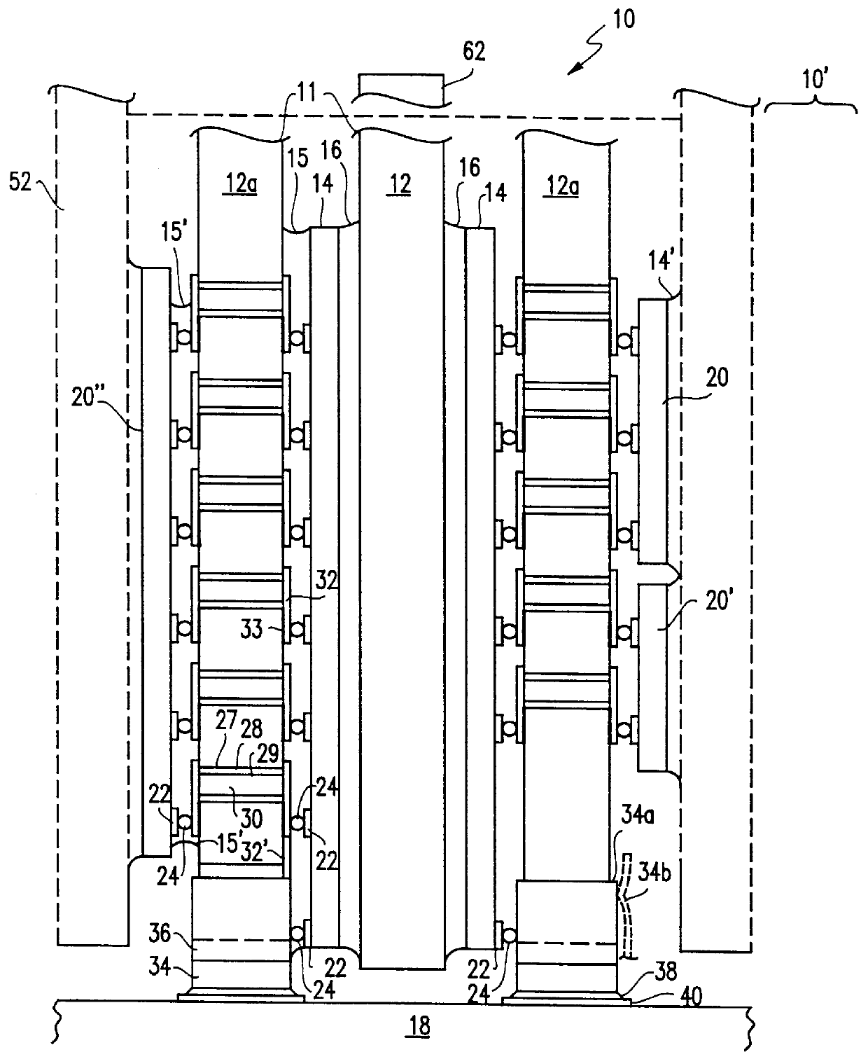
Referring now to the drawings, and more particularly to FIG. 1, there is shown, in cross-section, a preferred packaging structure 10 in accordance with the present invention. In this exemplary form of the invention illustrated in FIG. 1, three heat sink lamina 12, 12a, preferably formed of a graphite composite material or fiber / graphite matrix are shown. Other conductive materials of high thermal conductivity such as metals (e.g. copper, silver, aluminum, etc.), chemical vapor deposited (CVD) diamond, aluminum nitride, copper beryllium alloys or copper aluminum nitride alloys can be used in the practice of the invention as well.

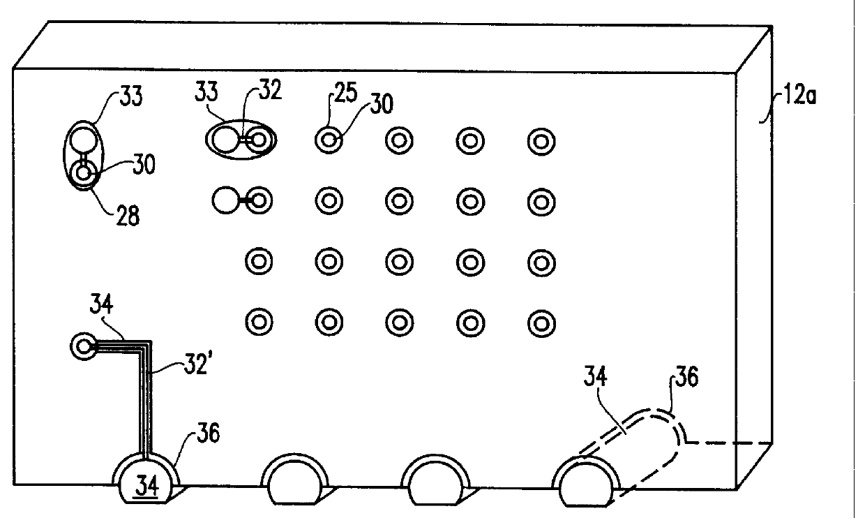
In this particular case, heat sink lamina 12a provides through connections 30 between major surfaces thereof made in a manner which will be discussed in greater detail below while lamina 12, as illustrated, does not. It should be understood that, as package and circuit designs may dictate, through connections 30 may be included in any or all such lamina 12, 1...


PUM


Abstract

Electrically conductive lamina are attached by an electrically insulating, thermally conductive adhesive and/or solder to one or more semiconductor devices such as chips and extend beyond the periphery of the chip or chips to form heat sink fins. Electrical connections may be made between such chips through holes (e.g. by a wire or plated through hole) in the electrically conductive lamina lined with an insulating material such as the electrically insulating adhesive to provide a structurally robust assembly. Surface pads and connections may overlie patterns of insulator on the lamina. A further lamina can be wrapped around lateral sides of the assembly to provide further heat sink area and mechanical protection for other heat sink fins. A graphite/carbon fiber composite matrix material is preferred for the lamina and the coefficient of thermal expansion of such materials may be matched to that of the semiconductor material attached thereto. Conductivity of the lamina also provides shielding against electrical noise to improve the noise immunity of short connections between chips made through the lamina as well as that of surface connections which may be formed on the lamina.

Description

1. Field of the InventionThe present invention generally relates to packaging of semiconductor devices formed on multiple chips and, more particularly, to the manufacture of a modular device with plural semiconductor chips including high power devices and / or high performance, high-density processors, memories, application specific integrated circuits (ASICS) and logic devices.2. Description of the Prior ArtIt has long been recognized that reduction of size of circuit elements and reduction of spacing and length of connections therebetween in integrated circuits and electronic packages containing one or more integrated circuit chips provides both economies of manufacture and performance improvements. Reduced size of circuit elements generally provides reduced parasitic capacitance and inductance and improved switching speed. Closer spacing of circuit elements on chips, especially in combination with reduced circuit element size, provides potentially increased functionality of each ch...

Claims


Application Information

Patent Timeline
Patent Type & Authority Patents(United States)
IPC IPC(8): H01L23/34H01L23/48H01L23/538H01L23/52H01L23/498H01L23/373H01L23/58H01L25/065
CPCH01L23/3733H01L23/49805H01L23/5384H01L23/585H01L25/0657H01L2225/06517H01L2224/16225H01L2225/06541H01L2225/06551H01L2225/06589H01L2224/16227H01L2224/73204H01L2224/73253H01L2225/0652H01L2224/05573H01L2224/05568H01L2224/056H01L24/05H01L2924/00014
Inventor INGRAHAM, ANTHONY P.KEHLEY, GLENN L.SATHE, SANJEEV B.SLACK, JOHN R.
Owner GOOGLE LLC
Why Eureka
Try Eureka